The EZ-USB FX20 is a programmable USB controller supporting speedy transfers via USB 20Gbps and LVDS interfaces. It is the latest addition to Infineon’s EZ-USB line designed to add USB connectivity to devices with high-performance requirements in AI, image processing, and other demanding applications. It offers up to six times the bandwidth of its predecessor, the EZ-USB FX3.
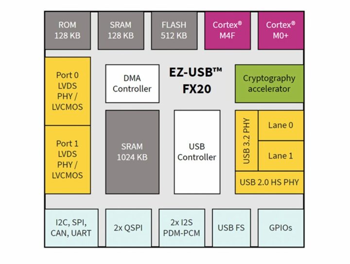
The FX20 is powered by a dual-core MCU subsystem, with ARM Cortex-M4F and ARM Cortex-M0+ cores. It features 512KB flash, 128KB SRAM, 128KB ROM, and seven serial communication blocks (SCBs). The cryptography accelerator and high-bandwidth data subsystem enable Direct Memory Access (DMA) data transfers via the supported interfaces. The programmable USB controller includes 1MB of SRAM for USB data buffering.
EZ-USB FX20 specifications:
- CPU – Dual-core, ARM Cortex-M4F core@ 150 MHz, ARM Cortex-M0+ core @ 100 MHz
- Memory – 512KB flash, 1024 + 128KB SRAM
- USB – USB 3.2 Gen 2 x2 device port
- Integrated PHY: 10 Gbps (x1/x2), 5 Gbps (x1/x2), 480 Mbps
- USB-C plug orientation detection and correction
- Peripherals
- Dual mode high bandwidth data interface
- LVDS / SubLVDS: up to 16 RX data lanes at 1.25 Gbps
- LVCMOS: up to 32-bit data bus at 160 MHz DDR
- I/O ports
- 2x Quad-SPI (QSPI)
- 7 serial communication blocks (I2C, SPI, CAN, UART)
- USB Full-Speed (12 Mbps) device
- 2x I2S/PDM-PCM and GPIOs
- Dual mode high bandwidth data interface
- Cryptography accelerator
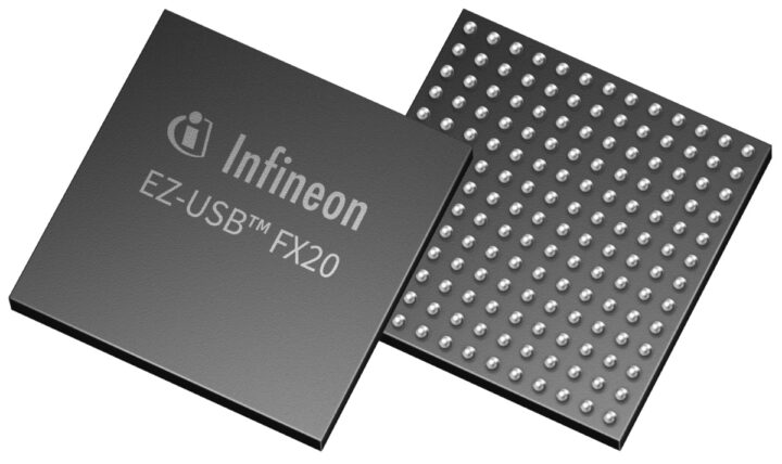
- Package: 10 mm x 10 mm, 169-ball, 0.75 mm ball pitch

The EZ-USB FX20 device integrates USB-C port orientation detection and supports direct USB-C connection without a signal multiplexer, simplifying design and integration. Infineon provides a quick-start development kit that includes firmware and a configuration tool. It includes a standard FPGA Mezzanine Card (FMC) connector for connecting the device to FPGA cards for programming/debugging. Also, there are application notes for hardware and software design to ease development and reduce time to market.
The programmable USB controller comes in a 10 x 10 mm² BGA package for BOM optimization and is ideal for space-constrained applications. Development samples are currently available for the FX20 and the device is scheduled for full release in Q1 2025. It is available in two variants: the CYUSB4024B0 model has all the features described above while the CYUSB4022B0 version lacks the LVCMOS alt mode, QSPI interface, and crypto accelerator. More information about the FX20 is available on the product page and press release.
Thanks to TLS for the tip.

Tomisin is a writer specializing in hardware product reviews, comparisons, and explainers. He is very passionate about small form factor and single-board computers.
Support CNX Software! Donate via cryptocurrencies, become a Patron on Patreon, or purchase goods on Amazon or Aliexpress


