Stefano Viola’s NiCE5340 SoM is built around a Nordic Semi nRF5340 Bluetooth SoC, an iCE40 FPGA, 11 sensors, a battery charger, and various other peripherals in a 29×16 mm form factor. The nRF5340 used in the SoM is a low-power, dual-core Arm Cortex-M33 SoC with Bluetooth 5.4, Bluetooth LE (BLE), Thread, Zigbee, and other proprietary protocols. Meanwhile, the Lattice iCE40 FPGA features 3520 logic cells, 80 Kbits of embedded Block RAM, I2C, and SPI blocks, and many other features that make it suitable for applications like environmental monitoring, health tracking, and others.
Previously, we have written about Unexpected Maker NANOS3, TinyS3, FeatherS3, and ProS3 boards, and ESP32-S3 4G dev board which all fall under the tiny and compact board category but this is the first time we have seen an MCU board with so many features built into a module of that size.
Stefano Viola’s NiCE5340 SoM Specification
- ICs
- Nordic Semiconductor nRF5340 dual-core Arm Cortex-M33, Bluetooth 5.4 SoC
- Lattice Semiconductor iCE40UP5K-UWG30 FPGA
- Storage – 64Mbit (8MB) flash (AT25QL641-UUE-T)
- Wireless Connectivity
- Bluetooth 5.4 LE (BLE)
- Thread
- Zigbee
- Sensors
- 6DOF IMU – LSM6DSMTR (STMicroelectronics)
- Biosignal converting unit – AS7057-BWL (Osram)
- Magnetometer – MMC3630KJ (Memsic)
- SAR sensor (touch) – SX9328ICSTRT (Semtech)
- PDM MEMS MIC – ICS-41351 (TDK)
- Humidity/temperature – SHTC3 (Sensirion)
- Haptic driver – DRV2605LYZF (Texas Instruments)
- RGB IR color sensor – BH1749NUC-E2 (Rohm Semi)
- Barometric pressure sensor – DPS310XTSA1 (Infineon)
- Charge/discharge current measurement – INA231AIYFDT (Texas Instruments)
- Misc – RTC – MAX31342EWA+T (Analog Devices)
- Power Management – Nordic Semiconductor nPM1100
- Additional Features:
- Onboard chip antenna
- MHF4 connector for external antenna
- RGB LED (Only the R and G connected)
- Dimensions – 29 x 16 millimeters
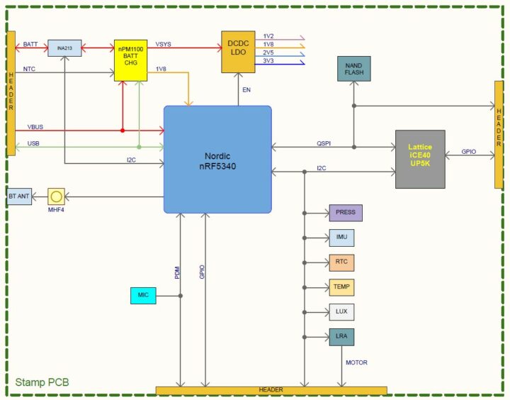
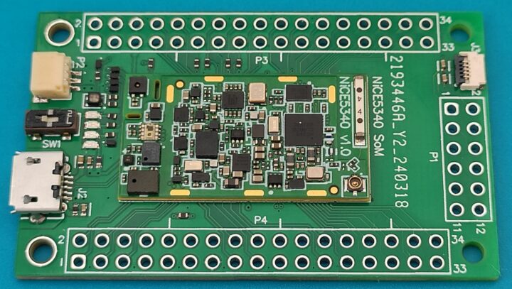
After a careful inspection, I immediately noticed that there was no way to program this board so after looking at the schematic of the board I found that there is a separate carrier board for the SoM, and there, the USB port is directly connected to the nRF5340 IC, and the SoC is connected to the FPGA via I2C and QSPI bus. As the nRF5340 is a wireless IC, Viola mentioned that it can also support Over-the-air (OTA) programming but OTA for the FPGA is still in the testing phase.
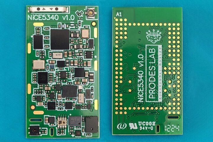
Upon checking I found the design of the SOM is quite unique and annoying at the same time, The SoM will not feature a connector like Raspberry Pi CM4 or a SODIMM connector like the Late Panda Mu, but the SoM has land-grid-array (LGA)-style pads which need to be reballed and then soldered to the carrier board.
Stefano Viola designed the NiCE5340 board primarily as a design challenge, so its future isn’t set in stone. You can find the PDF schematic and nRF5340 firmware on GitHub, and Viola plans to add code examples for the Arm MCU and iCE40 FPGA soon. If you’re interested in this board, want to try it out, or have ideas for improvements, connect with Stefano Viola on LinkedIn.
by Hackster.io
Debashis Das is a technical content writer and embedded engineer with over five years of experience in the industry. With expertise in Embedded C, PCB Design, and SEO optimization, he effectively blends difficult technical topics with clear communication
Support CNX Software! Donate via cryptocurrencies, become a Patron on Patreon, or purchase goods on Amazon or Aliexpress


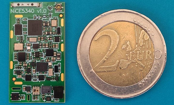


It’s a good idea to have placed a coin next to it. Everything on the board is so small that it in fact looked like a regular, much larger board without the coin!
> but this is the first time we have seen an ESP32(-S3) board with so many features built into a module of that size.
Note that this is not an ESP32-based board at all. Nordic is a completely different vendor. Quite interesting, nonetheless, but programmed using a vastly different ecosystem.
Sorry, my mistake, I was not thinking right when editing the post.
sorry again! My brain went ESP mode while comparing this SoM against so many ESP devices.
Thank you all guys.
Perhaps the SoM has an unusual electrical connection, but its small size does not allow for other possibilities.
The aim was to design a module that was miniaturised enough for wearable applications as well.
The header is LGA and the use of the SoM involves a small mainboard for the final application.
I am well advanced with the bring up and the power consumption is very low.
Almost all the peripherals were tested individually.
The future goal is to be able to create a dashboard where I can collect all the data from the various peripherals via BT.
I hope to get the help from some friends who are kindly contributing to the repository.
Unfortunately I am very limited in terms of code, so any help will be welcome.
Thanks
Great work Stefano Viola. We would like to try Zephyr RTOS with this and support in terms of software. Happy to discuss.
I hope to see a Pip-Boy or Tricorder very soon!