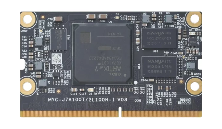
MYIR MYC-J7A100T is a System-On-Module (SoM) powered by an AMD/Xilinx Artix-7 XC7A100T FPGA with up to 101,440 logic cells, 512MB DDR3 memory, 32MB QSPI FLASH, 32KB EEPROM, DC-DC power management, and other integral circuits in a compact 69.6 x 40mm form factor.
The module exposes up to 178 FPGA I/Os, four pairs of GTP high-speed transceiver interfaces, and a JTAG interface through its 260-pin edge connector. MYiR also provides a development board for the MYC-J7A100T module which looks like a PCIe 2.0 card and comes with SFP+ cages, HDMI input and output ports, dual GbE, and a GPIO expansion header.
MYIR MYC-J7A100T system-on-module
Specifications:
- FPGA – AMD/Xilinx XC7A100T Artix-7 FPGA (XC7A100T-2FGG484I) with
- 101,440 logic cells
- 4,860 Kb of Block RAM
- 240 DSP slices
- 8 GTP transceivers capable of reaching speeds up to 6.6Gb/s
- PCIe Gen2 x4 interface
- Up to 300x single-ended I/Os
- System Memory – 512MB DDR3
- Storage – 32MB QSPI Flash, 32KB EEPROM
- Carrier board interface – 260-pin edge connector
- 178x programmable I/Os
- Bank 13 – 35 I/Os
- Bank 14 – 45 I/Os
- Bank 15 – 48 I/Os
- Bank 16 – 50 I/Os
- MGTP – 20-pin for high-speed serial interfaces
- JTAG Debug
- 178x programmable I/Os
- Supply Voltage – 5V, 3A recommended
- Dimensions – 69.6 x 40mm (12-layer PCB design)
- Temperature Range – 40 to 85 Celsius (industrial grade)
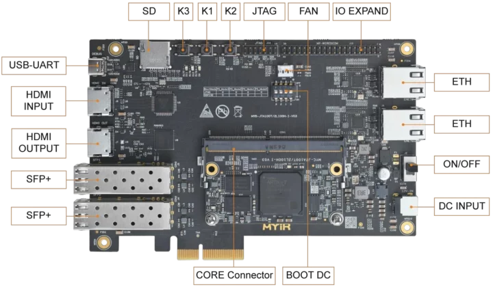
MYIR MYD-J7A100T AMD XC7A100T FPGA development board
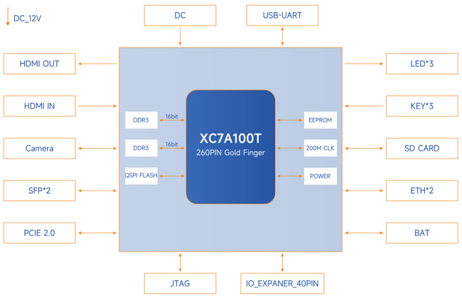
The company also provides the MYD-J7A100T development board fitted with the MYC-J7A100T SoM and offering the following interfaces:
- 260-pin socket for MYIR MYC-J7A100T system-on-module described above
- Storage – MicroSD card slot
- Video Interfaces
- HDMI input and output
- DVP digital camera interface with support for MYIR’s MY-CAM011B 2MP camera module
- Networking
- 2x SFP+ cages
- 2x Gigabit Ethernet RJ45 interfaces
- Expansion
- PCIe 2.0 interface
- 40-pin male expansion header for MY-WIREDCOM RPI module adding RS232/RS485 interfaces
- Debugging – JTAG; USB-to-UART interface via USB Type-C port
- Misc
- 3x buttons
- 3x LEDs
- 1x DIP switch for Boot selection and Power On/OFF
- Power Supply – 12V/2A via DC power jack
- Dimensions – 167.64 x 130.65mm (6-layer PCB design)
- Temperature Range – -40 to +85 Celsius

Software, price, and availability
MYiR Tech provides a range of Vivado sample codes for testing purposes from a basic LED blinky to more complex HDMI input/output, PCIe, and SFP+ test programs. The company will not typically make those public and only provides software resources to paying customers.
It’s unclear why MYiR decided to launch Artix-7 FPGA at this time as the Xilinx (now AMD) XC7A100T FPGA has been around for many years, and we previously covered Trenz Electronic TE0725LP board in 2019 and the MicroNova Mercury 2 in 2020. We also wrote about a 3D game engine C to FPGA implementation running on Digilent Arty A7-100T board with the same XC7A100T FPGA.
The solution is said to be suitable for industrial control, automation, communication, computing, and other highly customized applications. MYIR MYC-J7A100T system-on-module and MYD-J7A100T AMD XC7A100T FPGA development board are available now for $125 and $169 respectively. More details, including hardware documentation and purchase links, can be found on the product page.

Jean-Luc started CNX Software in 2010 as a part-time endeavor, before quitting his job as a software engineering manager, and starting to write daily news, and reviews full time later in 2011.
Support CNX Software! Donate via cryptocurrencies, become a Patron on Patreon, or purchase goods on Amazon or Aliexpress


Despite the picture saying SFP+, this FPGA can only reach SFP (non-plus) speeds on the GTP transceivers (SFP+ is 10G, SFP is 1G)