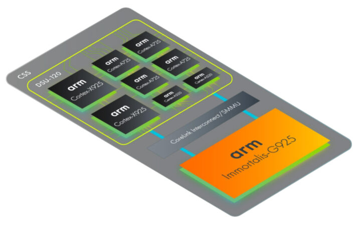
Arm has just announced new Armv9 CPUs and Immortalis GPUs for mobile SoCs, as well as the Kleidi AI software optimized for Arm CPUs from Armv7 to Armv9 architectures.
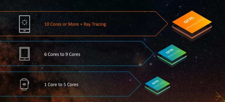
New Armv9.2 CPU cores include the Cortex-X925 “Blackhawk” core with significant CPU and AI performance improvements, the Cortex-A725 with improved performance efficiency, and a refreshed version of the Cortex-A520 providing 15 percent efficiency improvements. Three new GPUs have also been introduced namely the up-to-14-core Immortalis-G925 flagship GPU which delivers up to 37% 3D graphics performance improvements over last year’s 12-core Immortalis-G720, the Mali-G725 with 6 to 9 cores for premium mobile handsets, and the Mali-G625 GPU with one to five cores for smartwatches and entry-level mobile devices.
Arm Cortex-X925
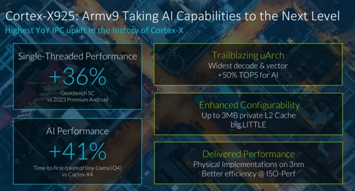
The Arm Cortex-X925 delivers 36 percent single-threaded peak performance improvements in Geekbench 6.2 against a Cortex-X4-based Premium Android smartphone, and about 41 percent better AI performance using the time-to-first token of tiny-LLama (Q4). The Cortex-X925 core was implemented on an FPGA platform with the following configuration: Cortex-X925 @ 3.8 GHz with 2MB L2 cache, 16MB L3, 32MB SLC, DSU @ 2 GHz, and LPDDR5x-8533 memory.
The AI performance was measured to be improved by 46 percent using the time-to-first token for Phi3, and Arm also says X925 SoCs can deliver 33 percent faster application launch times on average across five of the top 10 applications (in Android), and 60 percent faster web browsing measured using the Speedometer 2.1 browser benchmark. The slides shared by Arm mention support for Android, Linux, and Windows operating systems, so it will not only be used in smartphones but also mobile and AI PCs.
The Arm Cortex-X925 core is optimized for 3nm manufacturing processes. You’ll find more technical details about the new core on the developer’s website.
Arm Cortex-A725 and improvements for the Cortex-A520 core.
The Cortex-A725 further improves the performance and efficiency compared to the Cortex-A720 and Cortex-A78 cores. The new core delivers a 35 percent performance efficiency boost over the Cortex-A720, a 25 percent better power efficiency, and 20% L3 traffic improvements. Performance efficiency is defined as the ratio between the improvement in Performance and the improvement in Power for the said performance. The Cortex-A725 peak performance was apparently measured on a 3nm test chip with 64KB K1 and 8MB L3 caches, and compared to a 4nm Cortex-A720 chip. Besides the different process nodes, Arm claims most of the improvements to performance efficiency are due to the microarchitecture of the Cortex-A725.
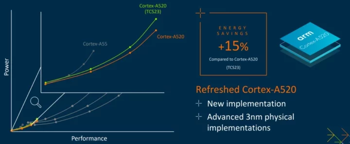
The Cortex-A520 has been refreshed with updated implementation and a 3nm process delivering up to 15 percent efficiency improvements compared to Cortex-A520 in TCS23.
Immortalis-G925, Mali-G725, and Mali-G625 GPUs
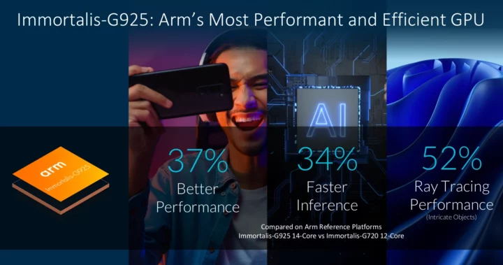
Like the Arm Cortex-X925 CPU, the Immortalis-G925 offers significant performance improvements over the previous generation Immortalis-G720 with 37% better performance in graphics apps, 34% faster AI inference (testing in fp16 mode), and 52% faster ray tracing. Arm further states that the Immortalis-G925 GPU delivers 46 percent performance improvements in mobile, on average, compared to the Immortalis-G720. Some examples include Genshin Impact with a 49 percent boost and Roblox which is 46 percent faster, and the company also tested Call of Duty Mobile, Diablo Immortal, the Day After Tomorrow, Fortnite, and PUBG Mobile with improvements ranging from 29 to 72 percent. We’re also told efficiency has improved by 30 percent on average in leading games.
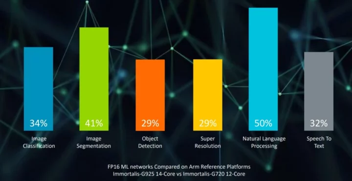
Immoratlis-G925 AI performance improvements with image classification, image segmentation, object detection, natural language processing, and more…
Arm did not expand on the Mali-G725 and Mali-G625 GPUs. Those look to be smaller variants of the Immortalis-G925 with fewer cores and now ray tracing capabilities optimized for mid-range and entry-level devices.
Kleidi AI software
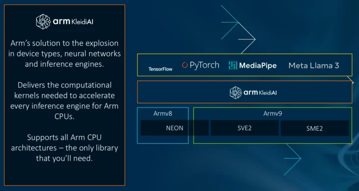
Arm Kleidi is a suite of software libraries and developer communities designed to accelerate AI development. The Arm Kleidi libraries support popular AI frameworks and are optimized for Arm CPUs from the Armv7 architecture using the Advanced Single Instruction Multiple Data (SIMD) Extension for machine learning (ML) workloads up to the new Armv9 architecture with more advanced features enabling generative AI workloads on the Arm CPU.
Kleidi is comprised of two main projects for now: KleidiAI for neural networks and inference engines and KleidiCV for OpenCV computer vision library.
KleidiAI is a collection of highly optimized AI kernels that work through MediaPipe (via XNNPACK), LLAMA.cpp, PyTorch (via ExecuTorch), and TensorFlow Lite (via XNNPACK). Arm says KleidiAI can accelerate the time-to-first token for Meta’s Llama 3 and Microsoft’s Phi-3 LLMs using llama.cpp by 190 percent on the new Arm Cortex-X925 CPU compared with the reference implementation based on llama.cpp. KlaidiAI is also being integrated into Unity Sentis on-device AI inference engine for game developers
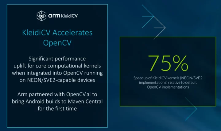
KleidiCV is developed in partnership with OpenCV to optimize over 2500 computer vision algorithms in the popular open-source library. NEON/SVE2-optimized implementations deliver a 75 percent performance uplift on average. Android builds are also being submitted to the Maven Central repository of open-source software components and libraries for Java development
You’ll find a few more details about Kleidi in the announcement.
All those new IP blocks and software make the Arm Compute Subsystems for Client (Arm CSS for Client) that will be integrated into SoCs for AI PCs, smartphones, consumer devices, and more. We’ll likely have to wait until 2025 at least before the first devices with Arm Cortex-X925 or Cortex-A725 come to market.

Jean-Luc started CNX Software in 2010 as a part-time endeavor, before quitting his job as a software engineering manager, and starting to write daily news, and reviews full time later in 2011.
Support CNX Software! Donate via cryptocurrencies, become a Patron on Patreon, or purchase goods on Amazon or Aliexpress


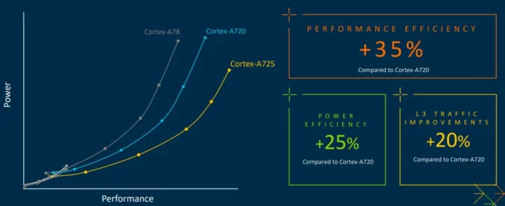


I love how Arm’s marketing team consistently draws comparative graphs with no scale to demonstrate the better performance of their new CPU. I’m sure they’re using the same graph year after year and just changing the CPU names.
Another point that’s missing is the comparison with commonly available cores. They could have displayed A76 or even A72 that attendees can compare to RPis and that would be even more impressive. At least they did it with the A55, showing the refreshed A520 could be twice as fast in the same power envelope.
Well, as you pointed out the graphs miss the scale. You don’t know if the x axys is at zero or if the graph is even in a linear scaled way. The comparison A55 vs A520 could well mean 15% higher performance at same power envelope but including advancements of litography.
Overall I find the development of the lower end of ARM CPUs to be a continueing disappointment for serveral years now. ARM is close to a stand still while everyone around is moving fast and even Intel is starting to dip into a similar perf/power with their low power -mont CPUs. And Intel rivalilng in terms of efficiency tells it all.
> even Intel is starting to dip into a similar perf/power with their low power -mont CPUs
What are you talking about? Intel’s TDP nonsense?
intel cores are not bad at all, they just suck a lot of power at high frequencies and since they design them for high frequencies, they make them operate to the max. I wouldn’t be surprised if an N100 was 3 times faster than an A55 at the same frequency, meaning that an N100 at 600 MHz could match an A55 at 2 GHz. If so, it could be very likely that the 600 MHz one would suck less power. A55 are very good in terms of efficiency, they’re about the limit of what can run without a heat sink. But I tend to think that an x86 core such as those found in N100 could run without heat sink at 600 MHz as well.
> I wouldn’t be surprised if an N100 was 3 times faster than an A55 at the same frequency
More like (a little less than) twice as fast. And by talking about N100 you somehow confirm that Intel’s marketing BS works since while N100 has the silliest TDP rating (6W at 800 MHz) it is not the most energy efficient Alder Lake-N thingy being sold 🙂
[ “the silliest”, sorry, but anyone ever benchmarked what’s the influence of pop up windows on cpu/gpu(maybe even npu with current hardware and libraries enabling all) with cookie consent requests and while disallowing ‘legitimate interest’ check boxes on the hundreds?
That’s where ‘silliest’ for hardware tech’s vs. software ‘marketing’ influences started? (some of it improved, but not everywhere, dp. POV)
(We would need someone programming these things telling about their motivation, for their/that POV, also)?)
increased demand for software expansions (e.g. memory above 4GB limit years ago, 32 to 64bit) on hardware lost some of it’s attraction, compared to previous (more substantial?) progress?
It’s an A76 or a X3 or a X925, nice, but on processes and consumer programs POV there’s fewer limitation without knowing that (compared to A17 (ARM Cortex, not Apple A17) vs. A72/A73 era)?
ISA instruction adjusting maybe? ]
The problem precisely is their marketing BS, because no single CPU nowadays consumes as much as 6W at 800 MHz. It certainly covers GPU, DDR controller, PCIe controller and whatnot in fact, which is a bit comparing apples and oranges when we compare to other SoCs used headless and without PCIe for example. That’s why it’s more difficult than just advertising a single integer number of watts, and I think they’re just englued in this stupid process that consists in showing SKUs, frequencies, prices and TDP ranges. They should probably instead use new approaches such as “zero cooling solution”, “small passive heatsink”, “large massive heatsink”, “small fan”, “large fan”, “water cooling”, “custom-designed cooling solution”. When you see how difficult it is nowadays to convince a hardware maker to take certain CPUs for 1U servers, they’re basing their arguments on these bogus TDPs and when you insist and show them that 50% higher TDP than they accepted stays perfectly cool, they’re simply surprised. These numbers are just making it harder for final users to get the CPUs they need for a given purpose.
[ what includes another difficulty with highly performant SoCs: being on battery management within phones there’s a balance between user accepted wait times (excluding network delays within comparison) and additional power increase on high(est) clock speeds;
It will take reviews on phone systems for getting experience on that trade of between improved battery systems (capacities?) or improved SoCs efficiencies (including additional hardware sections&accelerators), later than ’25, if products (an real consumers usage profiles, on average) are available.
PCIe is a real interest, if version 3 or 4 with more than 4 available lines are available for external devices (apart from phones), but that’s (at least) another 2 yrs into the unknown times?
and an idling 10&-cores GPU efficiency, waiting for mainline Kernel support? ]
My point was a different one. Here are all the Alder Lake-N SKUs, their burst frequencies and their TDP ratings at completely different and completely irrelevant ‘Base Frequencies’:
* N50: 2 cores, 3400 MHz / 6W @ 997 MHz
* N95: 4 cores, 3400 MHz / 15W @ 1700 MHz
* N97: 4 cores, 3600 MHz / 12W @ 2000 MHz
* N100: 4 cores, 3400 MHz / 6W @ 800 MHz
* N200: 4 cores, 3700 MHz / 6W @ 1000 MHz
* N300: 8 cores, 3800 MHz / 7W @ 800 MHz
* N305: 8 cores, 3800 MHz / 15W @ 1800 MHz
Everyone loves N100 since ‘so efficient’ while the opposite is true. We had this discussion already a year ago.
Well, maybe based on your table above the N100 is made from the poor bins and the good ones are reserved for N97 or N200, I don’t know. My point is not about N100 specifically but modern x86 low-end cores, which are gaining in efficiency when Arm is gaining in performance but not fast enough to catch up with low-end x86 (I’m not speaking about the fast cores like Apple’s M1/2/3). With that said, the I/O on RK3588 are pretty decent and that may compensate for the slower cores on various workloads.
I think ARM’s real sin is that the core comparison ends up being a node comparison, despite some of the cores supposedly being node independent (Cortex-A76 can be found on 7/10/16 nm, last one being the Pi5).
Is a Cortex-A725 really 35% more efficient than Cortex-A720? No, some if not most of that is coming from moving from a 4nm node to 3nm.
Marketing departments doing marketing things. I really wonder why anyone is paying attention to this BS.
because to the consumer its irrelevant where the efficency gains come from.
To see how efficient an “old” arch can be, just look at the steam deck, the zen2 cores in there hold their own against zen4 just by being manufatured on a modern node.
I wish intel made a sandy bridge die using tsmc 4nm. At 6mm2 these quad cores would be tiny, then again even back then half the area was for the igpu…
The original Steam Deck is on TSMC N7 like most Zen 2 cores in existence, and the refresh went to N6. I don’t think N6 vs. N7 matters that much. Steam Deck does well against the Zen 4 APUs because it’s a well balanced custom chip intended for lower power use. AMD’s off-the-shelf mainstream APUs (e.g. Phoenix) have more CPU cores and higher clocks than gamers actually need, and the ROG Ally et al. can run hot to get better 1080p performance.
AMD is going to have a lot of interesting options with Zen 5 APUs: top-end Strix Halo mega APU using chiplets and up to a 256-bit memory controller; high-end mainstream Strix Point with 4x Zen 5 cores, 8x Zen 5C cores, 16 CUs; the smaller Kraken Point with 4x Zen 5, 4x Zen 5C, and 8 CUs; and Sonoma Valley with 4x Zen 5C and likely weak graphics as a replacement for Mendocino.
Out of all of those, Kraken Point and some form of Strix Halo retaining the 256-bit memory bus while skimping on the core count could be best suited for handhelds. If Steam Deck 2 gets a custom chip, it ought to use low power ‘C’ cores, whether that’s Zen 5C or Zen 6C. They will be more than enough for a gaming handheld.
Intel doesn’t need to make a shrunken Sandy Bridge quad-core. They have relatively small 8-core Gracemont E-core dies with the IPC of Skylake and lower clocks (Alder Lake-N). Recent reporting suggests that there will be a massive IPC boost for Skymont E-cores, burying anything that came before it.
You should pay attention to Intel’s upcoming Lunar Lake APUs (TSMC N3B+N6 nodes), which could be great in every way with the probable exception of the price. And if we see a successor to Alder Lake-N using 8 Skymont cores, that could be a big hit in the x86 mini PC/SBC market. I just wish they bring back dual-channel memory.
Lots of typos, Immoralis, COrtex, etc. FWIW
Would love to see a Armv9 SBC that has a GPU that matches. The RK3588 is a great SoC where the GPU seems to manage 75% of what the CPU can manage with ML in a very general way.
Maybe a 4.2 big.Little or 8.4 and a match gpu and have less emphasis on a NPU due to how propreitory they can be with current software and frameworks.
I think also as you scale up to that level ram modules than soldered on could be preferential.
Likely the 1st Armv9 SoC based SBC of the approx $100 point will make it an instant curiousity buy to play with.
More stuff that we wont use until 2030 with luck! great thanks ARM!