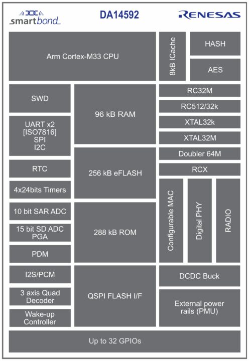
The DA14592 System-on-Chip (Soc) is Renesas’ “lowest power consumption and smallest, multi-core Bluetooth LE device.” According to the company, this chip’s design was achieved by making careful tradeoffs between on-chip memory and die size.
The chip offers an ultra-low power mode that uses only 2.3mA when transmitting radio signals at 0dBm and consumes 1.2mA to receive radio signals. It also supports a hibernation mode that uses about 90nA and can extend the operating life of battery-powered products. The active mode is best for processing-intensive products and uses 34µA for every MHz of CPU clock.
Projected key applications for the DA14592 chip include crowd-sourced location (CSL) tracking as used in Apple’s Airtags, remote control units, human interface devices, asset tracking, IoT end nodes, data logging, connected health, and activity tracking.
Renesas DA14592 specifications:
- CPU cores:
- Cortex-M33F running at up to 64MHz as application core
- Cortex-M0+ at 64MHz as configurable MAC
- Memory:
- Embedded Flash – 256KB
- RAM – 96KB RAM (+16KB cache)
- ROM – 288KB (including boot ROM, PKI routines, and Bluetooth® LE stack
- QSPI PSRAM/Flash interface
- Wireless
- Standards – Bluetooth 5.2 LE and 2.4GHz proprietary
- Configurable transmit output power: -18 to to +6 dBm
- -97 dBm receiver sensitivity
- Single wire antenna – no RF matching or RX/TX switching required
- High-performance mode – TX output: -22 to +6 dBm, RX sensitivity: -97 dBm
- Low-power mode – TX output -23 to 4.5 dBm, RX sensitivity: -96 dBm
- Peripherals
- Audio
- PDM interface with hardware sample rate converter
- I2S/PCM master/slave interface up to eight channels
- 32x General Purpose I/Os
- 8-channel 10-bit SAR ADC, 2 Msamples/s
- Delta-sigma (ΣΔ) ADC, 15 bits at 1 ksps, 13 bits at 16 ksps with a Programmable Gain Amplifier (PGA)
- 2x UARTs up to 3 Mbps, one UART extended to support ISO7816
- 1x SPI+ and 1x I2C controller at 100 kHz, 400 kHz, or 3.4 MHz
- 3-axis capable Quadrature Decoder
- 1x Real Time Clock with 10ms resolution
- 4x general-purpose, 24-bit up/down timers with PWM capabilities
- Audio
- Security – Application cryptographic engine with AES-256 and SHA-256
- Power/Clock management
- Buck converter
- Hibernation (Shipping mode) < 100 nA
- Programmable thresholds for brownout detection
- 32 MHz or 64 MHz system clock using a doubler
- Fast wake-up from sleep in <15 μs
- Power consumption
- RadioRx = 1.2mA, RadioTx = 2.3mA
- Active = 34uA/MHz, Hibernation = 90nA
- Package
- WLCSP39, 2.48 x 3.32, 0.42 mm diagonal pitch
- FCQFN52, 5.1 x 4.3 mm, 0.4 mm pitch
The previously released DA1470x SoC shares several features with this new Renesas chip but has a dedicated 2D GPU & display controller for GUI applications. We also recently covered Renesas’ new Cortex-A55 microprocessor targeted at IoT edge and gateway devices.
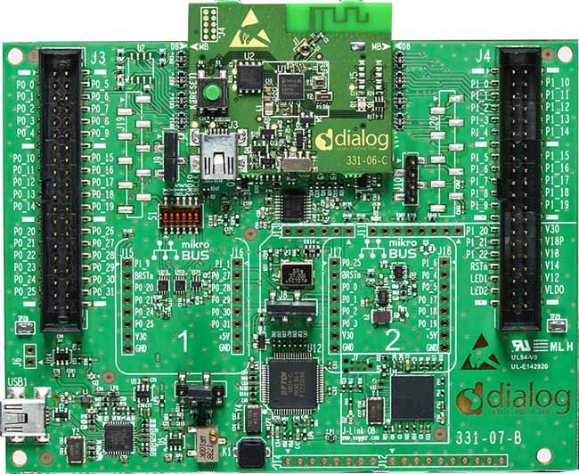
Renesas has also announced an associated system-on-module, the DA14592MOD, featuring “all external components required to implement a Bluetooth LE solution.” A development kit for the SoC can be ordered from the product page and includes a motherboard, daughterboard, and cables. Also, more information about the DA14592 can be found on the product page, including a datasheet, release notes, manuals, and guides.
The DA14592 is currently in stock and can be bought for $4.35 per chip (with bulk discounts available). The module, however, is pending regulatory certification which should be granted around the second quarter of 2024.
Via Hackster.io

Tomisin is a writer specializing in hardware product reviews, comparisons, and explainers. He is very passionate about small form factor and single-board computers.
Support CNX Software! Donate via cryptocurrencies, become a Patron on Patreon, or purchase goods on Amazon or Aliexpress


