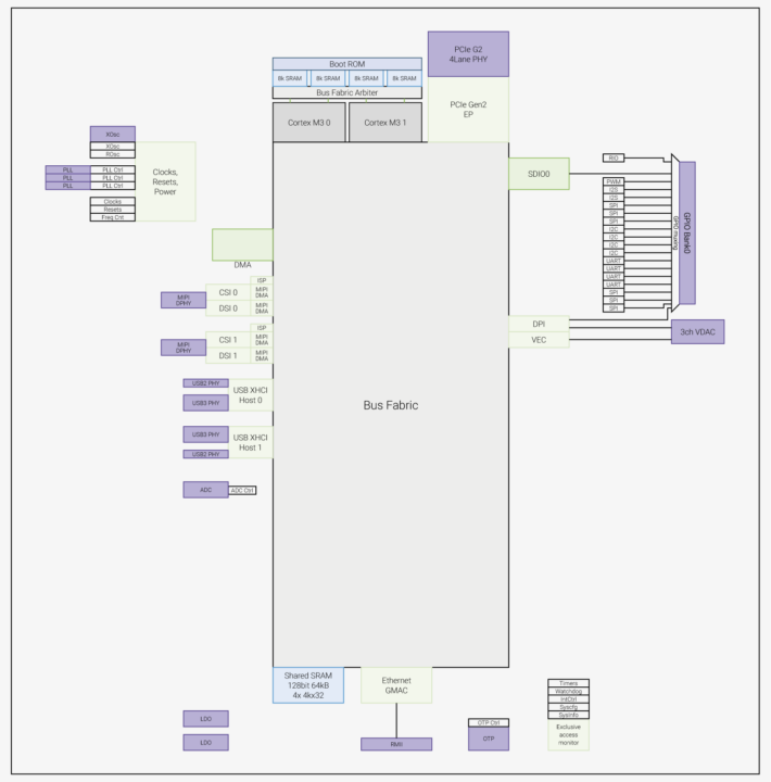
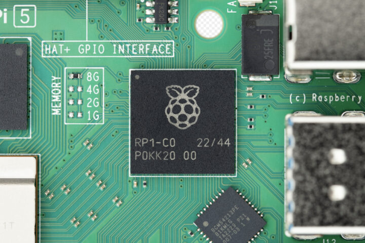
The Raspberry Pi 5 was recently introduced with the Broadcom BCM2712 CPU and the RP1 chip handling I/Os designed in-house by the Raspberry Pi just like they did for the RP2 (RP2040) microcontroller, and we now have more details about the Raspberry Pi RP1 including a (draft) datasheet and a block diagram.
The RP2040 came out before the RP1 peripheral controller as the design for the latter started 7 years ago with a total R&D budget to develop the Raspberry Pi 5 of around 25 million dollars. While at launch, we knew the RP1 handled some peripherals, doubled USB bandwidth with two separate USB 3.0 hosts, and embedded higher speed MIPI interfaces, it was unclear whether some of the other connections came from the BCM2712 or RP1 chips. But we now do know with the release of the datasheet.
Raspberry Pi RP1 key features and specifications:
- MCU – Dual-arm Cortex-M3 microcontroller with 64KB SRAM, TCM, bootROM for platform configuration and management
- Host interface – PCIe 2.0 x4 bus
- MIPI camera/display interfaces
- 2x MIPI CSI-2 camera controllers and 2x MIPI DSI display controllers connected to 2x shared 4-lane MIPI DPHY transceiver PHYs for up to 8 Gbps bandwidth.
- Each camera controller incorporates an image signal processor front-end (ISP-FE) which pre-processes incoming image data.
- Possible configuration include 2x cameras, 2x displays, or a one display + one camera
- Networking – Gigabit Ethernet MAC (RGMII)
- USB – 2x XHCI controllers each connected to a single USB 3.0 PHY and a single USB 2.0 PHY for up to 10 Gbps total bandwidth (5Gbps per XHCI controller)
- GPIOs
- 28x GPIO pins
- 5V tolerant, and 3.3V-failsafe (supports a voltage of up to 3.63V applied when RP1 is unpowered)
- GPIO alternate functions
- Storage – eMMC/SDIO bus with a 4-bit interface
- Display – 24-bit DPI output
- Audio – 2x I2S, stereo PWM audio output (AUDIO_OUT)
- 5x UART, 6x SPI, 4x I2C
- 4-channel PWM output
- Interrupt generation from pin level or edge transitions
- Clocks
- 1x Clock Producer instance
- 1x Clock Consumer instance
- General-purpose clock input and output (GPCLK)
- RIO – Registered IO interface to allow the host processor to manipulate GPIOs
- Misc
- 8-channel DMA Controller (DMAC) for servicing low-speed peripherals.
- 3x integrated PLLs consisting of 2 fractional-N PLLs to support the generation of independent video and
audio clocks, and 1x integer PLL to generate system clocks. - A five-input successive-approximation analog-to-digital (ADC) converter with 12-bit resolution at 500kSPS with
9.5 ENOB (Effective number of bits), 4 external inputs, one internal temperature sensor
- Dimension – 20mm² die
- Process – TSMC’s 40LP (Note: the BCM2712 is manufactured with a 16nm process)

There’s no mention of flash storage for the firmware, but Eben Upton explains the datasheet release is only partial and aimed at developers implementing drivers for the Raspberry Pi 5 SBC. It also looks like the Raspberry Pi RP1 may have some hidden (i.e. yet-to-be-publicly-documented) features as we’re told “while we are looking at exposing more of the features of RP1, both in software and with further documentation, that’s going to be something you might see a little later on”.

Jean-Luc started CNX Software in 2010 as a part-time endeavor, before quitting his job as a software engineering manager, and starting to write daily news, and reviews full time later in 2011.
Support CNX Software! Donate via cryptocurrencies, become a Patron on Patreon, or purchase goods on Amazon or Aliexpress


[ comparable to earlier x86(_64) ‘Southbridge’ controllers, nowadays Intel’s Chipset (e.g. ICH_-2008, now PCH ‘platform controller hub’ ~14nm(IceLake or 10th_gen Core i, >=470/480/490&server&mobile) ) or AMD’s Fusion controller hub (FCH_-2016, now AM4 ~14nm, TRX40/WRX80, AM5) ?]
Since the 40-pins connector is connected to the RP1 I wonder if (like with the RPI4) it is still possible to power the RPI5 from the 40-pins (for UPS functionality).
There is the increased power consumption (if not 5A than probably more than 3A during start with network and SSD) and the question if an RP1 can be fed from the 5V and GND pins from the header. I believe Eben mentioned the 40um RP1 was also to be used as buffer between the RP1 and the more vulnerable parts.
I only scanned the document but could not find any information on power lines.
Just think about shape and connectors of their new PoE-HAT für the RPi 5B and you know that 5V/GND pins on the GPIO header are not connected to RP1 but to the PMIC. But in this case even with PoE+ you need to adjust a setting to ramp up current on the USB3 ports.
While almost anyone fears insane consumption increases their 5V/5A PSU attempt is mostly there to avoid undercurrent on the USB3 ports (undervoltage seems to be a different story and I’m really surprised that none of the reviewers so far had a look at it).
[ saw a number for a USB-C 240W USB4 cable, marked EPR, having ~120mOhm (GND30&VBUS90)mOhm resistance for ~1.2m (another cable ~0.5m ~90mOhm), what’s a voltage drop each 1m ~0.3-0.5V on 3-5A current supply (?) ]
As for what Mr. Upton mentions and what not you should keep in mind that he’s CEO and marketing guy.
If it’s true they started already in 2015 with RP1 maybe at that time BroadCom’s STB division’s roadmap looked like ‘VideoCore EOL soon’ so RPi Trading Ltd. had to address this painfully/slowly implementing an I/O chip providing RPi compatible low-speed and high-speed I/O to be paired with whatever PCIe capable SoC in the future?
Want to post your list of the known IP blocks in the RP1?
Well, not really interesting other than searching for various quirks with certain controllers: https://github.com/geerlingguy/sbc-reviews/issues/21#issuecomment-1751060564
But since they have the RP1 C0 stepping out since at least Feb 2022 I would assume they could iron out a lot of problems on the software side in the meantime (talking about USB3 issues especially).
This looks more like a desktop PC.
If you’re not talking about RPi 5B but RP1 instead… then quite the opposite: this RP1 I/O chip is a mandatory companion to current VideoCore SoCs since 1.5 decades ago those VC SoCs were used in phones, media players, iPods. The available interfaces followed the use case and RPi implemented many of them.
Current VideoCore SoCs from BroadCom’s STB department are only media players any more and lack a lot of stuff (e.g. h.264 decoder, video encoders, MIPI, USB3). RP1 to the rescue.
Again no other SBC manufacturer offers such an advanced south bridge for the I/O.
Probably other manufacturers don’t have the issues thar Rpi5 has with I/O LOL
This is designed to reduce manufacturing cost rather than provide “advanced io”. If you pay a little bit more, you can get richer IO with SoCs like RK3588 and get all the IOs on the SoC. You don’t have to pay more is the point of having this bridge chip.