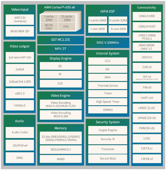
Allwinner A523 is an octa-core Cortex-A55 processor clocked at up to 1.4/1.8GHz in big.LITTLE (DynamIQ) configuration and mainly designed for tablets with multiple display interfaces such as two 4-lane MIPI DSPI interfaces, two MIPI CSI camera interfaces, a Mali-G57 GPU, and more. But the block diagram below also shows two Gigabit Ethernet (GMAC) interfaces and HDMI 2.0 output among other interfaces meaning it will likely be used in Smart Home products as the Allwinner R828/MR828, and possibly automotive products as the Allwinner T527.
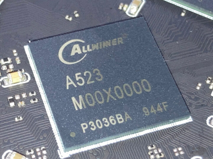
I first discovered the Allwinner A523 last March via a tweet by (GLGH_), but there was little information at that time. We now have further details about the processor and upcoming products such as the Teclast P26T, and a potential Allwinner A523 single board computer or module.
Allwinner A523 preliminary specifications:
- CPU
- Application – Octa-core Arm Cortex-A55 @ in big.LITTLE configuration with four cores @ 1.80 GHz and four cores @ 1.42GHz
- Real-time – E906 RISC-Vcore @ 200MHz
- GPU – Mali G57 MC1 2EE
- DSP – HiFi4 audio DSP
- NPU – 2 TOPS AI accelerator
- System Memory – 32-bit DDR3, LPDDR3, DDR4, LPDDR4, or LPDDR4X 2400MHz
- Storage I/F – MMC, eMMC 5.1, SPI Flash
- Video output
- Internal – 2x RGB, 2x MIPI DSI, dual-channel LVDS, 1x eDP1.3 up to 2560×1600 @ 60Hz
- External – HDMI 2.0
- Camera – 8M ISP, 2x 4-lane MIPI CSI
- Audio – Audio codec, 4x I2C/PCM, DMIC
- Networking – 2x Gigabit Ethernet (GMAC)
- USB – 1x USB 3.0 (apparently multiplexed with 1-lane PCIe 2.1), 2x USB 2.0
- PCIe – 1-lane PCIe 2.1
- Other peripheral interfaces
- SDIO 3.0
- 2x CAN Bus
- 4x SPI (also used for NAND/NOR flash)
- 9x TWI/I2C, 10x UART
- 2-ch LRPADC, 24-ch GPADC
- 30x PWM
- 1x CIR Tx, 2x CIR Rx
- Security system – Crypto engine, security ID, TrustZone, secure boot
- Process – 22 nm
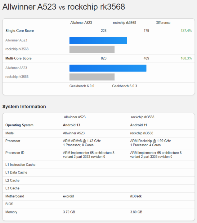
The specifications above are derived from information from the block diagram above and linux-sunxi community since Allwinner has just to publish information about the new processor. Some of the details conflict, so there may be errors. The Arm Cortex-A55 CPU frequencies come from Geekbench 6 results shared by GLGH_, which compare the Amlogic A523 to the Rockchip RK3568 (4x A55 @ 1.99 GHz) and show noticeable performance improvements in terms of CPU performance somehow even for the single thread benchmark despite the higher frequency.
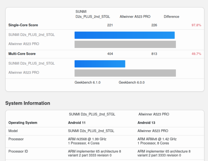
It must be an outlier as if we select other Geekbench 6 results, both have a similar single-core performance. One difference is the use of Android 13 against Android 11, but I’m not sure it matters that much for those types of CPU benchmarks.
One of the first products based on Allwinner A523 is the Teclast P26T tablet with a 10.1-inch IPS display with 1280×800 resolution, 4GB RAM, and 64GB eMMC flash, but currently only sold in China. GLGH_ also plans to work on a new project based on the new octa-core Cortex-A55 project, which probably means a module and/or single board computer is in the works, or soon will be.


Jean-Luc started CNX Software in 2010 as a part-time endeavor, before quitting his job as a software engineering manager, and starting to write daily news, and reviews full time later in 2011.
Support CNX Software! Donate via cryptocurrencies, become a Patron on Patreon, or purchase goods on Amazon or Aliexpress




So Allwinner has finally renewed their license and is no longer limited to 20th century cores ? That’s good news. What’s a bit less good is that they managed to set two distinct frequencies depending on the cluster, like amlogic used to do with its A53 long ago. But at least they’re back from the dark ages, let’s see how that evolves.
They almost certainly sacrified one cluster frequency so that it would take less area. It’s very common for tablets/phones SoCs to have those dual cluster of little cores with different frequency
I don’t see how it’s possible that the lower frequency one takes less area, what counts is the transistor counts and the process. At best they can save on power by using a fixed different voltage for each cluster but I would find it odd.
Why would transistor count and process be the only thing? What ARM gives to it’s client is usually the RTL, i.e. the functional description of the processor, the client is then usually responsible to do the physical implementation of it.
In the physical implementation, there are many choices you can make that impact performance vs area. You can see the semianalysis article on Zen 4C for details.
But just as an example of why it matters. Supposed you have an addition circuit(say for an ALU) that you need to be able to have X MHz with it. You start with a ripple carry adder, but that’s slow and you can only get up to Y MHz(where Y is smaller than X) so instead you use a carry select adder which can fulfill the necessary frequency.
The carry select adder however is a considerably bigger circuit(in fact, it needs two two ripple carry and mux). So if there is somewhere with lower performance needs(like say a cluster with reduced frequency) and Y MHz would satisfy it, you could user the slower circuit(but better area-wise) instead.
There is a lot of stuff like that, like High Density vs High Perfomance flip flop macros for processes
I think the 2+6 SoCs look ideal for tablets, e.g. 2x A76 + 6x A55. Or A78 in the case of the Mediatek MT8188J.
On the opposite, I think that many small cores bring absolutely nothing and are purely a marketing choice to advertise a larger number of cores than the competitor: virtually no workload scales efficiently on many cores, so a single more performant core will always be faster AND more efficient than many small ones that compete for memory access and burn cycles waiting on spinlocks. However, small cores are great because they’re super efficient, so they’re nice to run lots of small background tasks. But if you reach the point where your background tasks are able to saturate even a single such core, it becomes a bottleneck and you’d rather migrate that to a larger one than try to add more small ones. I find that 2+2 and 4+2 solutions (e.g. S922X has 4xA73+2xA53) are way smarter in this regard, even if they’re less appealing for the marketing and sales departments.
The only reason to have that many little processors is if they are each optimized for a particular execution speed. As persondb pointed out, you can optimize the same logical core type for different performance/power levels. So, I can see 2 big cores, two speed optimized small cores, and two more power optimized small cores. You would generally only use one set at a time as well. UI would live on the big cores and OS/background tasks would live on the small cores depending on how much needs to be done(or how latency sensitive it is).
But, yeah, 8 A55’s is a bit silly even if it’s two different clusters optimized for different things. The difference here isn’t enough to justify the extra cores. I doubt that they’re *that* more power efficient. Better to throw in more cache or just make the chip smaller.
I’d also say that a human interactive device like a phone or tablet is a failure unless it has at least *one* big core. It’s going to be painful to use because of UI latency. Getting a lot done quickly isn’t just needed for big compute tasks, it’s critical for keeping latency in check. Any you really only need one of those big cores.
I think 1/2/2 or 2/2/2 are the most logical arrangements. I think the real problem you run into in pairing the small cores with the big ones is that–unless you want a lot of OS level pain (I’m looking at you Intel), you want the feature set of all the cores to be the same. That means if you have fancy vector instructions for the big cores, the little ones need to have it as well–it can be super slow–but you have to have it because a task moving from one core to another should have to look at the CPU caps on every task switch.
USB3 and PCIe being shown in one block might already hint at both being multiplexed?
22nm ????? this is ancient!
You are probably confusing this with Intel’s old 22nm FinFET process that has long been abandoned, or TSMC’s failed 20nm process. The current 22nm processes are state of the art for anyone who doesn’t want FinFET these days, be it for cost, power efficiency or US embargo reasons.
I suspect this is the chip that first showed up on the roadmap as T723 a few years ago, where it was mentioned that this was Allwinner’s first chip beyond 22nm.
Indeed, usually you don’t want to go to thin for efficient cores, because the leakage can easily represent a significant portion of the total consumption. Small processes are interesting for power-hungry cores. BTW we won’t see 8nm microcontrollers soon I guess 😉
I’m pretty sure cost efficiency is the problem with using newer nodes, not electron leakage. The newer nodes are still more efficient than the older ones.
probably 22nm soi.
Dont belive. Allwinner does not use cortex a53? Ha ha