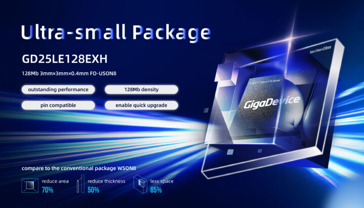
GigaDevice Semiconductor has just launched the GD25LE128EXH 128Mbit SPI NOR Flash in a tiny ultra-compact 3x3x0.4mm FO-USON8 package designed for IoT, wearables, healthcare, and networking products.
The GD25LE128EXH supports up to 133MHz frequency with four channels delivering up to 532Mbit/s data throughput. GigaDevice also highlights the low power consumption of just 6mA when reading, or a reduction of power consumption by 45% compared to previous devices.
GD25LE128EXH specifications:
- Density – 128Mb
- I/O Bus – Single I/O, Dual I/O, Quad I/O, QPI
- Frequency – 133 MHz (x1 x2 x4)
- Features
- H/W RESET
- WP#
- Security Registers with OTP Locks
- Suspend
- Unique ID
- HOLD#
- Voltage – 1.65V~2.0V
- Package – FO-USON8 3x3mm
- Temperature Range – -40°C~85°C; -40°C~105°C, or -40°C~125°C
The GD25LE128E SPI flash is also available in SOP8 208mil, USON8 4x4mm, WSON8 6x5mm, WSON8 8x6mm, and WLCSP (4-4 ball array) packages, which means the GD25LE128EXH’s FO-USON8 package reduces area by 70% and thickness by 50%, compared to the 6x5x0.8mm WSON8 package typically used for such products. Gigadevice also says the GD25LE128EXH takes up to 85% less space and reduces material costs.
Somehow, the 3x3x0.4mm FO-USON8 GD25LE128EXH is also pin compatible with 64Mbit and lower capacity 3x4x 0.6mm USON8 products from the family, enabling easy upgrades to 128Mbit without changing the PCB layout.
The GD25LE128EXH is currently in mass production, and another even smaller device is in the works with the 64Mbit GD25LE64E with a 3×20.4mm FO-USON8 package will start sampling by the end of the month. Additional information may also be found on the product page and the press release.
Thanks to TLS for the tip.

Jean-Luc started CNX Software in 2010 as a part-time endeavor, before quitting his job as a software engineering manager, and starting to write daily news, and reviews full time later in 2011.
Support CNX Software! Donate via cryptocurrencies, become a Patron on Patreon, or purchase goods on Amazon or Aliexpress


“Somehow”? Is that a machine translation artifact? SPI flash has had the same pin configuration for several decades now, so it’s not surprising that these chips would be the same. Quite the opposite, if they used a different pinout, that would be a very notable exception.
I just found it odd that packages with different dimensions would be pin-to-pin compatible.
Ahh, It’s pin compatable (which mean pin #1 on one package is pin #1 on the other), but not *footprint* compatable as in you can swap the packages out on the same board.
But here they say you don’t need to change your PCB layout to switch between the 3x4x0.6mm part and the 3x3x0.4mm part. I guess it’s possible, but I could not confirm it since they had not updated the datasheet with the new package at the time when I wrote about it.
I’m seeing the same thing. It looks like the 3×4 WSON-8 has a bunch of package that hangs beyond the pin outline, so you can draw a 3×3 square over the area where the pads actually are. That should make it compatable. The thickness doesn’t really effect this, so the x0.6mm or x0.4mm part doesn’t matter. It may effect other mechanical things with boards, but not the footprint.
Sort of sad that they haven’t updated the datasheet in a long time–over a year and a half ago.
That’s nice, because in some tiny projects, you can find that the common wide SOIC package used by such devices is quite large and can sometimes dominate the size of a small board.
M1S is one of those. Probably a lot of ESP32 modules.
Boards not effected: Pi Pico as it already uses an overly tiny chip considering how much empty board space it has.