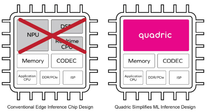
A typical chip for AI or ML inference would include an NPU, a DSP, a real-time CPU, plus some memory, an application processor, an ISP, and a few more IP blocks. Quadric Chimera GPNPU (general purpose neural processor unit) IP combines the NPU, DSP, and real-time CPU into one single programmable core.
According to Quadric, the main benefit of such design is simplifying system-on-chip (SoC) hardware design and subsequent software programming once the chip is available thanks to a unified architecture for machine learning inference as well as pre-and-post processing. Since the core is programmable it should also be future-proof.
Three “QB series” Chimera GPNPU cores are available:
- Chimera QB1 – 1 TOPS machine learning, 64 GOPS DSP capability
- Chimera QB4 – 4 TOPS ML, 256 GOPS DSP
- Chimera QB16 – 16 TOPS ML, 1 TOPS DSP
Quadric says the Chimera cores can be used with any (modern) manufacturing process and can achieve up to 1 GHz operation using 16nm or 7nm processes. Two or more Chimaera cores can be paired together for applications requiring more performance.

The Chimera GPNPU architecture is said to deliver ML inference performance similar to the efficiency of dedicated CNN offload engines, but with full programmability and the ability to run any ML operator, which may be critical if data scientists find better models requiring new operators that cannot run on existing fixed-function accelerators.
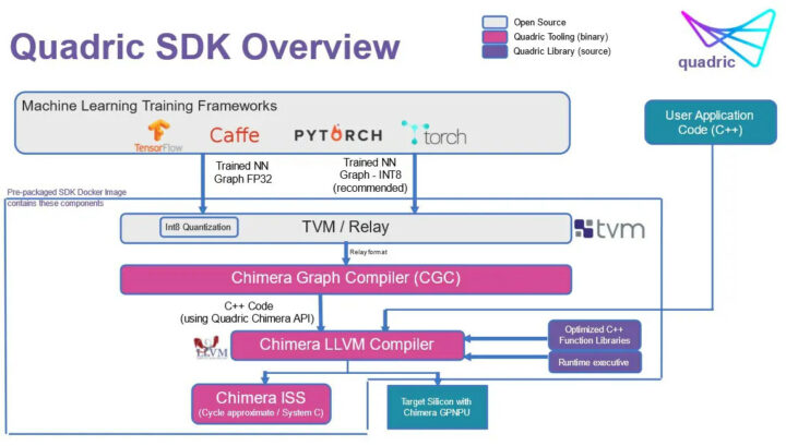
Quadric’s architecture combines the neural network graphs and C++ code into a single software code stream and only one toolchain is used for scalar, vector, and matrix computations. Memory bandwidth is also optimized by a single unified compilation stack that also helps lowering power consumption. Custom operators can be added by a software developer by writing a C++ kernel utilizing the Chimera Compute Library (CCL) API, then compiling that kernel using the Chimera SDK. The task of software engineers should be further simplified since they only work with one core and do not need to handle a multi-core heterogenous system.
It may take a while before the solution gets into actual chips, however. While the Chimera architecture has already been tested in silicon, Quadric is looking for customers whose chip design teams can start an IP evaluation this fall or winter, so I assume it may be a year or more before commercial SoCs based on the Quadic Chimera architecture become available. Additional details can be found on the products page and the press release.
Thanks to TLS for the tip.

Jean-Luc started CNX Software in 2010 as a part-time endeavor, before quitting his job as a software engineering manager, and starting to write daily news, and reviews full time later in 2011.
Support CNX Software! Donate via cryptocurrencies, become a Patron on Patreon, or purchase goods on Amazon or Aliexpress


That’s an interesting choice. Has the fraction of ML done at the edge gone that high that it pays to have no general purpose computing at all? Even an M3 type of core to coordinate things? DSPs became slightly less bad microcontrollers by adding bit manipulation instructions (back in the 90’s). Have they gotten that much better or is this chip just ‘not for those jobs’?
I’m very curious to see where this finds a home.
I think this is a FPGA type core which can reconfigure itself between ML, DSP and GP modes. They are using TVM which has a special back end for creating FPGA models matched to the gates available.
I am skeptical if this will be better than three optimized processors which can run in parallel.
Thanks for the clarification and I agree with you. From a power and performance standpoint, FPGA wins out over a general purpose processor in very specific applications, but custom ASICs beat FPGAs all the time. Maybe it has some fixed function blocks for DSP and NPU type of tasks and just used the FPGA to glue it all together most optimally for a given task.
Still, that seems like a loss to a small general purpose core coordinating an NPU and DSP (w/DMA, etc.). I remain curious.
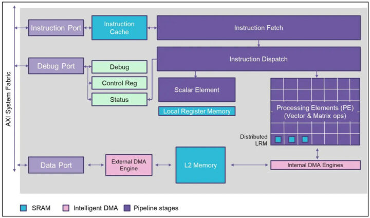
Looking at their block diagram more, it probably is CPU design which combines all three instruction sets DSP, ML and GP instead of the FPGA type.
Again I am not convinced this will beat a coprocessor architecture model.
This may be a decent edge computing design, but it is nothing revolutionary. Extensa architecture has had DSP instructions for years, I think they are adding ML ones.
If you look at the diagram, it looks like it might be way more parallel than DSP/ML vector instructions, close to a GPU or more like an memory array with simple ALU’s (IIRC, Micron looked into that a few years ago): look at the PE (processing elements) array with LRM (Local Register Memory).
In the past, I think people have found that model hard to program, so it hasn’t been successful.
Jon & David: Quadric CMO here. Thanks for the interest in our product. The Chimera processor is a hybrid between a modern DSP and a systolic array processor. Licensable IP delivered as source Verilog RTL – no funky FPGA fabric. Chip designers synthesize into vanilla standard cells in any process of choice. The architecture is a proprietary ISA. 64b instruction word, single issue per clock. The PEs are essentially 4 of the 7 stages of the execution pipeline with a massive amount of operand sharing and local storage. Chimera GPNPUs have significantly more DMA bandwidth than Xtensa cores and far greater compute capability than the vector-optimized DSPs from Tensilica that you referenced. Want more info? Visit our website: quadric.io.
Steve, Thanks for the summary! That description makes the block diagram make a lot more sense. Given this clarification, I can see how this architecture could be very flexable between DSP and NPU style tasks.
Such an arch would be very good at flexibly processing a variety of data manipulation heavy flows, but I still wonder how you handle mundane tasks like bit packing/unpacking that often dominate in embedded applications.
A stocastic array should be well suited to real time control processing, so that aspect of embedded computing shouldn’t be much of a concern. Oh, I also didn’t notice the application processor in the block diagram. I guess that would be tasked with such jobs.
For me what caused the confusion is the “realtime CPU” being crossed out and replaced with your IP. My brain saw “CPU” and generalized. It’s just the real time aspects of embedded control that get replaced, so something like a M3F core running control loops is more the target rather than a bit packing/unpacking, logic tree kind of embedded CPU task. That makes a lot more sense.
So, in summary, I didn’t understand the diagram well and it looks like this is an interesting variant on what’s been tried for embedded ‘edge’ (I hate that term) computing. It’s a little less hardcoded than having a DSP and NPU, but should still be able to handle the same tasks–depending on how the elements in the stocastic array work. With that kind of arch, it’s pretty easy to handle different word sizes, so smaller values for the NPU task and larger word sized for DSP (which always suffers from the speed/data size tradeoff).
My understanding after a brief reading of this design is that it’s basically the IP for a CPU (with proprietary CPU architecture) that has a whole 2D Systolic Array NPU effectively as a CPU instruction. That way it slightly reduces the overall silicon area needed for an SOC because there’s only one set of auxillary modules instead of 3 sets of aux modules needed for standalone CPU + DSP + NPU.
Did I understand it correctly? If so, I think it’s a good concept that might become popular in some form, but has the severe limitation of it being another proprietary CPU architecture. I imagine this would have made more sense to use a RISC-V based CPU, to have the benefits of the RISC-V ecosystem including optimising compiler and linker and libs, and maturity/longevity.
I’d like to start small and simple – an SDR with multiple modules (ie. Gnu radio). Run FFT, change FIR / IIR filter parameters in real time, etc. You don’t even need gigahertz sample rates, most spectrum in the hundreds of megahertz would be ample.
Deliberately lowering speed could bring a cheap sample to market faster, whetting our appetite for more powerful ersio s later.
Are you replying to the right article?