NXP i.MX RT500 is the second Cortex-M33 Crossover MCU following the NXP i.MX RT600 Series announced in 2018, and optimized for low-power HMI applications such as wearables and Smart Home & IoT devices.
NXP Crossover MCUs are typically clocked at 600 MHz or more, but NXP i.MX RT500 Cortex-M33 is limited to 200 MHz, and combined with 200 MHz Tensilica Fusion F1 DSP as well as a 2D GPU, and power optimizations that enable long battery life of up to 40 days on a charge for wearables like smartwatches.
NXP i.MX RT500 key features and specifications:
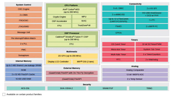
- MCU Core – Cortex-M33 @ up to 200 MHz with Arm TrustZone, M33 built-in Memory Protection Unit (MPU), PowerQuad hardware accelerator for DSP functions, CASPER crypto coprocessor for asymmetric cryptographic algorithms
- DSP Core – Cadence Tensilica Fusion F1 DSP @ up to 200 MHz
- On-Chip Memory
- Up to 5 MB of system SRAM accessible by both CPUs and DMA engines
- 2x 32 kB FlexSPI cache
- External storage I/F
- Quad/Octal SPI Flash with a dynamic description
- 2x SD/eMMC memory card interfaces including one supporting eMMC 5.0 with HS400/DDR operation
- Graphics – 2D GPU with vector graphics acceleration
- LCD interfaces
- 8/10/16/18/24-bit parallel LCD (FlexIO)
- MIPI DSI
- Camera – CSI 8/10/16-bit parallel (FlexIO)
- Peripherals
- 8-channel digital microphone interface
- 1x USB high-speed host/device controller
- Up to 12x FlexComm interfaces configurable as SPI/I2C/I2S/UART
- 1x SPI up to 50 MHz
- 2x I3C bus interfaces
- 12-bit ADC up to 1 Msps
- 2x 32-channel DMA engines
- Security
- Secure Isolation
- Secure execution environment through Arm TrustZone technology for ARMv8-M
- Symmetric key isolation through hardware engines
- Secure Boot
- Secure Storage – Physically Unclonable Function (PUF) based key store, On-the-fly-AES decryption (OTFAD) of off-chip flash for code storage
- Secure Debug – Certificate-based debug authentication mechanism
- Firmware update with authenticity (RSA signed) and confidentiality (AES-CTR encrypted) protection
- HW Crypto accelerators – 256-bit AES, TRNG with 256-bit entropy, SHA-256, and SHA-1
- 128-bit Universal Unique Identifier (UUID) and 256-bit Compound Device Identifier (CDI)
- Part of EdgeLock Assurance program
- Secure Isolation
- Package – FOWLP249, WLCSP141
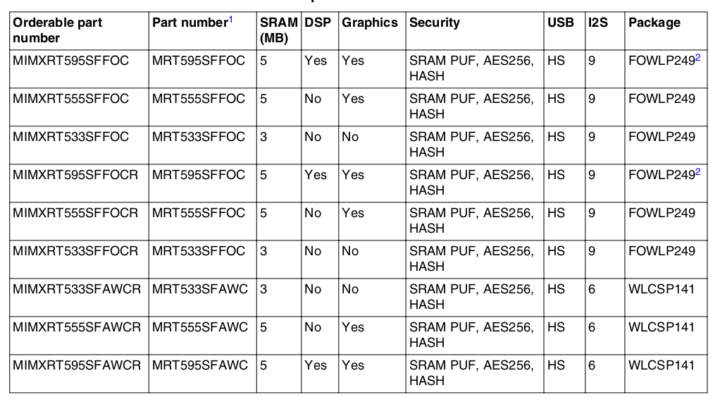 Looking at the datasheet, there appear to be three main parts with i.MX RT595 (DSP + GPU + 5MB SRAM), i.MX RT555 (GPU, 5MB SRAM, but no DSP), and i.MX RT533 (3MB SRAM, no DSP, no GPU).
NXP i.MX RT500 series microcontrollers are supported by the MCUXpresso SDK with LVGL open-source graphics library, and AI libraries are also provided with “eIQ Inference with TensorFlow Lite Micro” and the Voice Intelligent Technology (VIT) library for voice UI enablement with always-on voice detection and local commands. As we’ll see below, NXP i.MX RT500 MCU can also run FreeRTOS, and several other commercial solutions are offered.
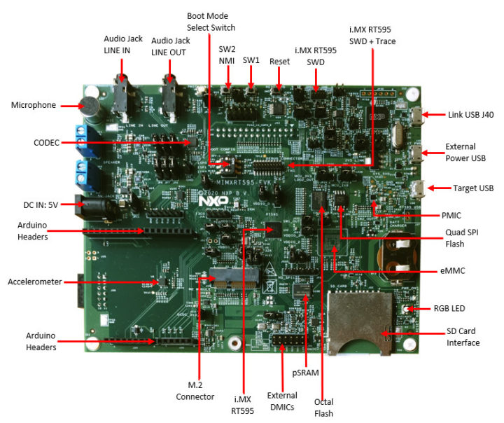
NXP has designed one development kit based on NXP i.MX RT595 crossover MCU with the MIMXRT595-EVK allowing developers to evaluate storage, display, and audio features of the new processor, optionally using Arduino shields, a 5.5-inch 1280×720 LCD display with touch-sensitive overlay, or a 1.2-inch circular touchscreen display with 390×390 resolution.
We can watch the evaluation kit fitted with the circular display in action below. The demo shows a user interface (Wearable UX) based on Crank Software’s Storyboard graphical toolkit, with the device running FreeRTOS open-source real-time operating system, and it’s pretty smooth for a 200 MHz device.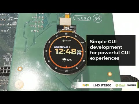
The first time I heard about the new NXP i.MX RT500 crossover MCU was from a press release from Microej that claims that “thanks to smart power savings core functionalities, smartwatches can now expect to achieve up to 40 days of autonomy on a standard battery”.
The announcement goes on to explain this is achieved by MICROEJ VEE’s platform with three optimization methods:
- Reduced active power with six different power modes that automatically adjust power consumption to save battery life (FULL, HIGH, LOW, SLEEP, SUSPEND and OFF). Power consumption is further reduces by automatic voltage adjustments and optimal RAM allocations.
- Reduced processing time by scheduling multitasking and synchronizing of timers, and all the generic library stacks (UI, IoT, etc.) have been re-designed to leverage the hardware execution units of the NXP i.MX RT500 MCU.
- Reduced standby power thanks to the built-in low-power modes of the new crossover MCU, and automatically reducing voltage while in the SUSPEND power state.
If you are interested in power management in NXP i.MX RT500, Alejandra Guzmán, System Engineer at NXP Semiconductors, has written a detailed article about the topic on All About Circuits.
NXP i.MX RT500 cross MCU has “limited availability” according to NXP, and indeed none of the distributors have stock with a typical lead time of 52 weeks (welcome to 2021!). MIMXRT595-EVK evaluation kit is sold for $129 and there are currently 16 units in stock. You’ll find more information including datasheets, software resources, and links to buy development tools on the product page.

Jean-Luc started CNX Software in 2010 as a part-time endeavor, before quitting his job as a software engineering manager, and starting to write daily news, and reviews full time later in 2011.
Support CNX Software! Donate via cryptocurrencies, become a Patron on Patreon, or purchase goods on Amazon or Aliexpress




Weird, why would devkit include 720p screen when built-in GPU’s hard limit is 640×480?
The answer is typical another failed product left a giant pile of unused screen in inventory.
I get that this is supposed to be chip for low-power smartwatches and it is killer for that – for now. We have already seen screen manufactures trading punches on prototyping better screens for wearables without resorting to OLED, once Apple goes beyond 480p (it is 368×448) others will follow. It does not matter for other chip makers like Ambiq (Apollo4 also has 480p hard limit) with shorter product cycles, but here, once RT500’s GPU gets obsoleted, there will be so much less use cases for the most of that chip’s lifecycle.