Lindenis V833 is an AI video/camera development board based on Allwinner V833 single-core Cortex-A7 processor with a 400 MOPS AI accelerator (NPU) and running OpenWrt-based Tina Linux or Melis RTOS based on the RT-Thread kernel.
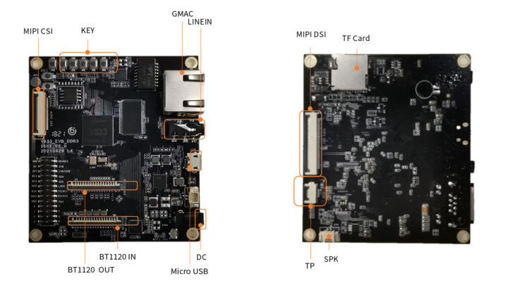
The board comes with up to 3GB RAM, a MicroSD card socket, MIPI DSI, MIPI CSI, and BT1120 interfaces for video output and input, Gigabit Ethernet, 2.4 GHz WiFi, and a few other I/Os.
Lindenis V833 specifications:
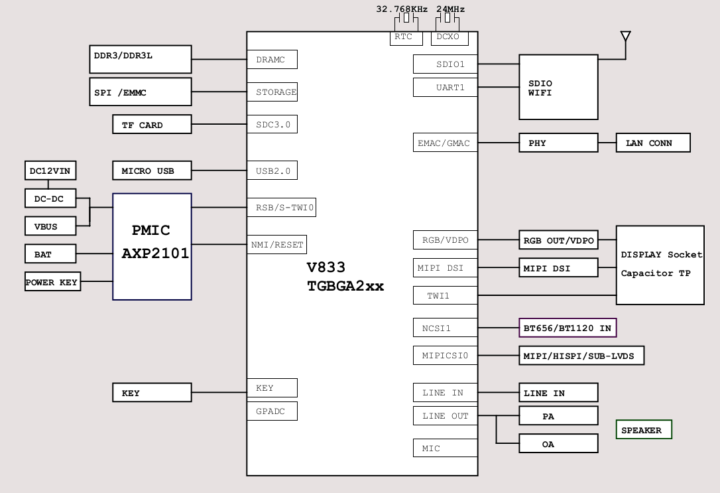
- SoC – Allwinner V833 single-core Arm Cortex-A7 processor @ up to 1.2 GHz with H.265/H.265 1080p video encoder, MJPEG 1080p video encoder, 400 MOPS AI accelerator (See PDF datasheet)
- System Memory – Up to 3GB DDR3/DDR3L
- Storage – MicroSD card slot with support for SDHC and SDXC, SPI NOR flash
- Display Interfaces
- 4-lane MIPI-DSI up to 1080p
- BT1120 output
- Touch panel header
- Video In
- 4-lane MIPI-CSI camera interface
- BT1120 input
- Audio – 3.5mm Line-in jack, built-in microphone
- Connectivity
- 10/100M Ethernet RJ45 port
- 2.4 GHz WiFi 4 via Allwinner XR819 module
- Expansion – 2x 13-pin header with I2C, I2S, PWM, GPIO, GPADC
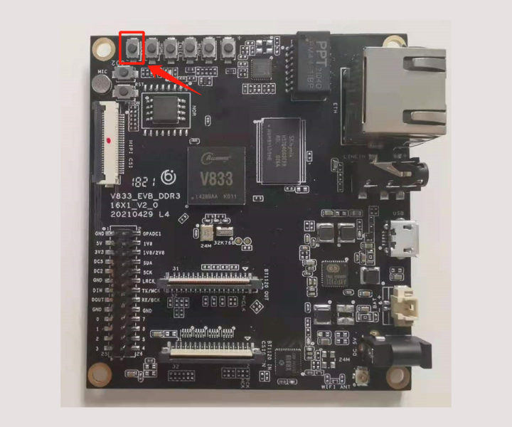
5V, 1V8, 2V8, and GND - Misc – Buttons for menu, volume, and firmware update, G-sensor (DA380),
- Power Supply
- 12V DC via DC jack
- 5V/2A via micro USB port
- 3.7V Li-Ion battery connector
- Dimensions – 75 x 68mm
 The Wiki provides hardware and software documentation including instructions to get started with Tina Linux (OpenWrt + Linux 4.9) or Melis RTOS based on the RT-Thread kernel. The company recommends Tina Linux as a video SDK is provided with a complete V4L2 framework and open-source applications/demos that include Lindlive low-latency streaming server,
Lindplayer video player, and Lindcamera camera app.
Note that some of the information is not very accurate, notably the memory and storage options are not clear, and it’s better to double-check the information using the schematic and other documents. You’ll also find several repositories on Github.
Allwinner V833 processor is similar to Allwinner V831 we previously reported on, but with a higher CPU clock (1.2 GHz vs 800 MHz), external memory support instead of on-chip DDR2, and a more powerful NPU (400 MOPS vs 200 MOPS). There’s also some reverse-engineering work taking place on Allwinner V831/V833 NPU to develop open-source tools.
Lindenis V833 is the third video/camera board using Allwinner V-series, with the company having previously launched the Lindenis H5 and Lindenis V536 (4K) camera boards, but with different form factors, so there’s no hardware/electrical compatibility between the boards.
Lindenis V833 development board can be purchased for $125 on Aliexpress, but again there’s no information about memory capacity and the type of storage soldered to the board.

Jean-Luc started CNX Software in 2010 as a part-time endeavor, before quitting his job as a software engineering manager, and starting to write daily news, and reviews full time later in 2011.
Support CNX Software! Donate via cryptocurrencies, become a Patron on Patreon, or purchase goods on Amazon or Aliexpress


What kind of display takes BT1120 for input?
My friend, in general, BT1120 will not input to the screen directly, but send video steam to video server via a cable. So v833 play a role of front TX in the whole data flow.
What’s the use cases for these boards? a smart edge AI video surveillance camera? an acceleration card for video analysis in a server rack?
The V831 is the follow on chip to the AW S3. The S3 sold many millions making those GoPro clone action cams. S3 is very old design and V831/3 is modern update. The AI unit is tiny. One use case for it would be to identify a person’s face in the view finder and then set the camera function to optimize the photo of the face. For hobbyist use — this is excellent, cheap chip for robotics. Think vision system for First Robotics.
If you want low cost, real AI video chip check out the RV1109/26. We are working with it and it can do real time object detection in the video stream. The RV11xx AI unit 10x+ faster than V831 one. But RV11xx is $10 and V831/3 is $3-4.
The Lindenis dev board is good deal for $115. It is professionally designed. The software will work. They will post all of the source code on github. And they will even answer a moderate amount of support questions. I would recommend developing on this board, and then if you want to make a dozen robots get a cheaper board like MAIX for the robot to use. Note that the Lindenis board is going to have a lot more RAM than the MAIX board which makes development tasks far easier.
Very interesting SoC which supports parallel RGB888 24bit lines for traditional TFT LCDs.
BTW, the type of storage soldered to the board seems to be Hynix H5TQ4G63EFR 512MB/4Gbit DDR3. It is very much smaller than 3GByte.
I suspect there’s simply another chip on the bottom of the board. This might be the 1GB model with twice 512MB, and the largest one might use 2+1GB. This might explain the apparent 3 DRAM chip layouts on the silkscreen.
@Willy, I couldn’t find any DRAM chip on the other side of the PCB.
The silkscreen just shows the different BGA package size options probably.
Since major Samsung & Hynix DRAM manufacturers discontinued 1GB/2GB DDR3 chips long time ago, it will NOT be feasible in the real world too.
Anyway, 512MB should be enough for those kind of application.
LPDDR3 can have much larger capacity including a 24Gbit package that allows a 3GB system with a single memory chip, maybe they support that for the higher capacities in addition to the 4Gbit DDR3?
It’s unclear whether the chip supports LPDDR3, as the datasheet only mentions DDR3, but the supported parts list that Jon linked to has LPDDR3 as well. From the silkscreen on the board photo, it does appear that two different package sizes are possible, but I don’t which types this corresponds to.
Supported RAM configurations. I don’t know which one they used.
http://files.lindeni.org/lindenis-v833/Documents/Hardware_Res/Support_list/Allwinner_V833_SDRAM_Support_List_V1.14.pdf
Hi my friends, I am a guy from Lindenis. Happy to see you all show much interest on our v833 Dev board.
If you have any questions, do not hesitate to e-mail me. I will try me best to help you.
Here are some typos in the article:
1. the power source voltage via DC Jack is 5V, not 12V.
2. v833 is a SOC focus on video encoding. So there is only hardware encoder module on chip, but no hardware decoder. So it cannot decode H.264/H.265 and MJPEG.
12V via DC jack was already there, and the rest of the power options is from your wiki (5V via micro USB and 3.7 LiPo battery).
I’ve corrected the specs to only show encoders, since indeed there are no decoders.
Dear Jean, thanks for your help firstly.
There is something wrong in our schematic that shows 12V power-in via jack, it should be 5V. I have fixed the typos and updated the schematic to the wiki. And please sync to you article later.
Thanks again.