We recently reported on the Rockchip developer conference (RKDC) 2020, and especially the upcoming Rockchip RK3588 Cortex-A76/A55 processor that packs a lot of power and features, and is now scheduled to launch in Q3 2021.
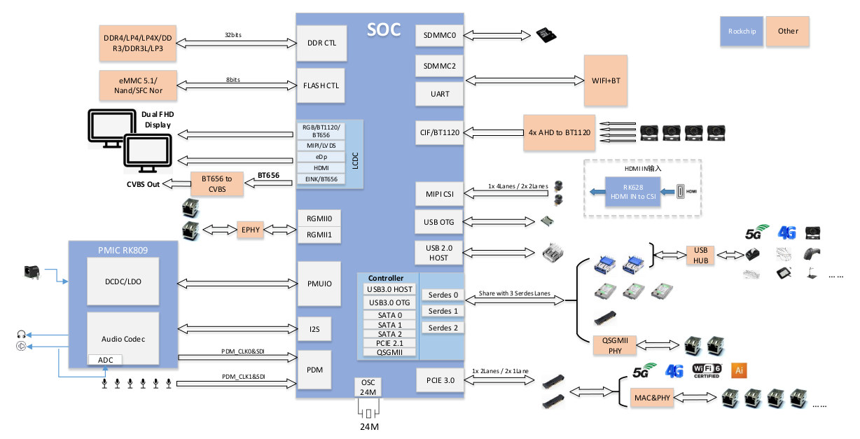
But as you can imagine there were other products revealed during the conference, including the new Rockchip RK3568, similar to the previously announced RK3566, and designed for edge computing and network video recorder (NVR) applications.
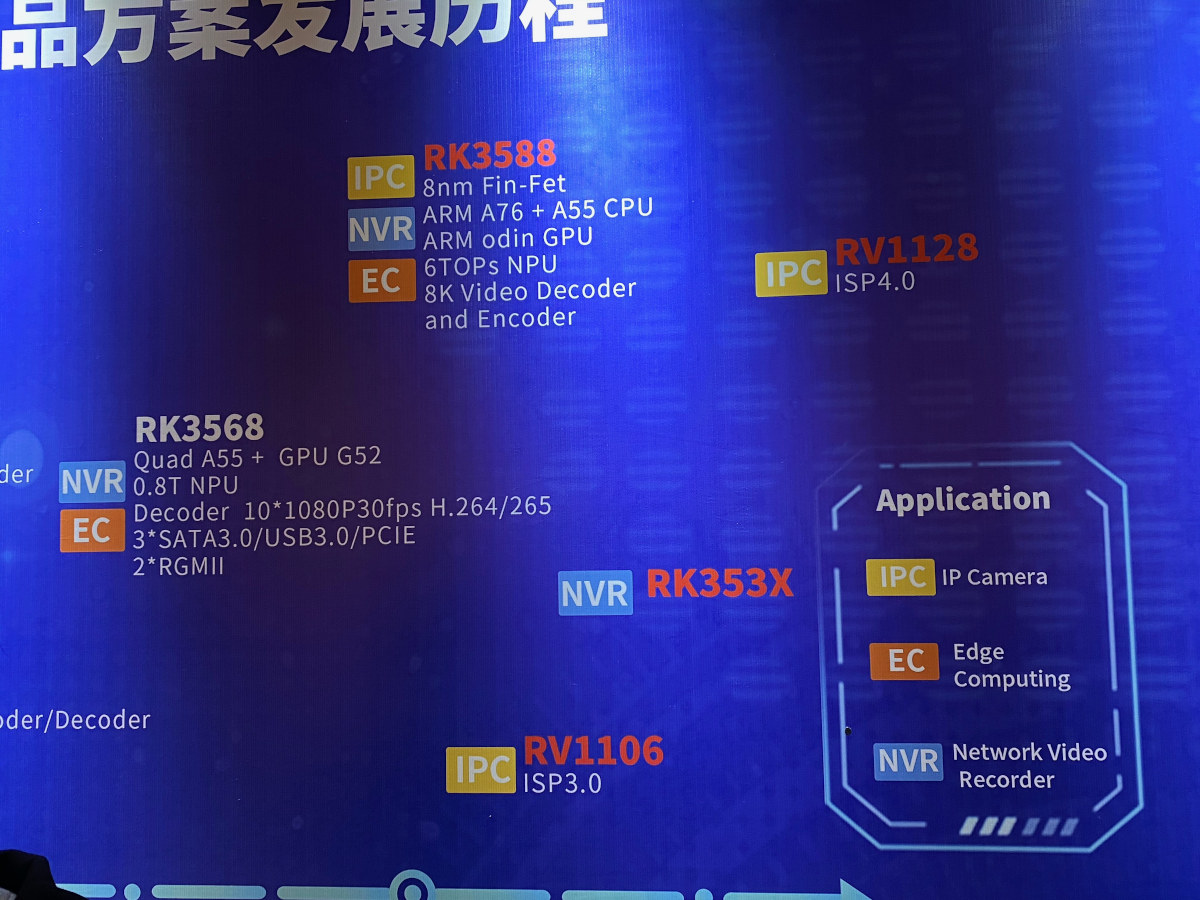 There’s also an RK353X processor specifically designed for NVR application that should have similar performance as RK3568, but a lower cost, as well as two UP camera SoC with RV1106 and RV1128.
CNX Software managed to obtain the presentation for the RK3568 processor from the conference so we’ll focus on the quad-core Cortex-A55 processor in this post.
Rockchip RK3568 specifications:
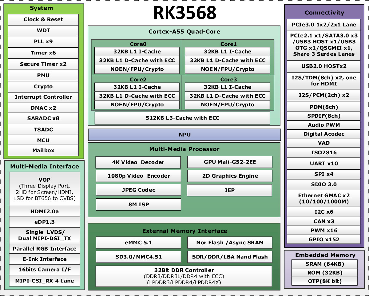
- CPU – Quad-core Cortex-A55 processor with NEON and FPU
- GPU – Mali-G52 EE with support for OpenGL ES 1.1 to 3.2, Vulkan 1.1, OpenGL 2.0
- AI accelerator – 0.8 TOPS RK NN accelerator @ up to 800 Mhz with 512x INT8 MAC, 128x INT16/FP16/BFP16 MAC
- Memory I/F – 32-bit DDR4/DDR3L/LP4/LP4x with ECC support
- Storage I/F – Nor SFC, SPI NAND, eMMC 5.1 , 3x SATA 3.0*, 8K OTP
- Display I/F – RGB, LVDS or MIPI DSI, HDMI 2.0a, eDP 1.3, e-Ink
- VPU
- Video decode – 4Kp60 H.264/H.265/VP9
- Video encode – 1080p60 H.264/H.265
- Camera
- 8M ISP with HDR
- 4-lane / 2x 2-lane MIPI CSI2 @ 2.5 Gbps per lane
- 16-bit DVP camera support with BT.656/601/1120
- Audio
- 8-channel I2S/TDM, 2x 2-channel I2S
- 8-channel PDM
- S/PDIF out
- Networking
- 2x Gigabit Ethernet (GMAC)
- Quad serial gigabit media
-independent interface (QSGMII)*
- USB – USB 2.0 host, USB 2.0 OTG, USB 3.0 OTG*, USB 3.0 host*,
- Other interfaces and peripherals
- 3x SDIO 3.0
- PCIe
- PCIe 2.1 1×1 lane*
- PCIe 3.0 1×2 lane or 2x 1-lane @ 8 Gbps
- 10x UART, 4x SPI, 16x PWM, 6x I2C, 3x CAN FD, 8x SAR-ADC
- Security – SM3/4 cipher, TEE, Arm Trustzone
- Package – TBD
- Process – 22 nm
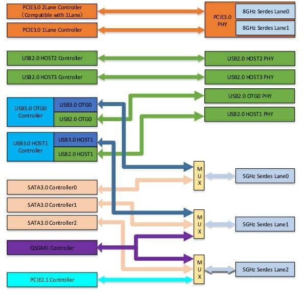
* USB3.0 OTG, USB3.0 HOT, SATA3.0, PCIE2.1, QSGMII are all multiplexed via
three Serdes lanes @ 5 GHz as shown in the diagram below.
Rockchip will provide Android and Linux BSPs for the AIOT processor, and the AI accelerator will support Caffe, TensorFlow, TF-Lite, ONNX, PyTorch, etc.. through the RKNN Toolkit already used by Rockchip RK1808 and RK3399Pro.
RK3568 is extremely versatile and Rockchip expects it to be found in NVRs, cloud terminals, IoT gateways and industrial control applications, car infotainment systems and dashboards, and even Karaoke machines.
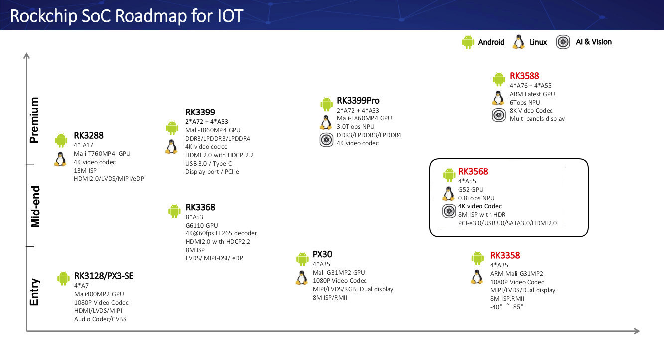
I was also informed that RK3566 specifications had changed a bit since the last announcement/leak in February, and now closely match RK3568 specifications except for the lack of PCIe 3.0 interface, and a smaller number of IOs. Both RK3568 and RK3566 are sampling now, and are sold as mid-range parts as shown in the Rockchip IoT SoC roadmap below which also reveals the new entry-level RK3358 quad-core Cortex-A35 processing coming soon.
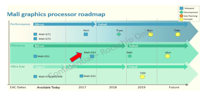
Those who follow RK3588 leaks history may remember the processor was first unveiled with an Arm “Natt” GPU, and in our recent story update, it got an upgrade to an Arm “Odin” GPU. Those are yet to be released Arm Mali “Vaxhall” GPUs, but a slide in the presentation show Natt is the successor of the mid-range Mali-G52, while “Odin” GPU are parts of the high-performance GPU such as Mali-G72…

Jean-Luc started CNX Software in 2010 as a part-time endeavor, before quitting his job as a software engineering manager, and starting to write daily news, and reviews full time later in 2011.
Support CNX Software! Donate via cryptocurrencies, become a Patron on Patreon, or purchase goods on Amazon or Aliexpress




The 0.8 TOPS NPU seems anemic compared to their A311D (5.0 TOPS, and actually available in the Khadas VIM3 for over a year) or a Coral device (4 TOPS). I imagine on those 10 streams you’d have to use it quite sparingly like frigate does: have a first pass that does simple motion detection, only do object detection on frames with motion, skip frames as necessary, and use a low-resolution model on just the portion of the frame where the motion occurs. Even then I’d guess it wouldn’t be enough, unless it’s somehow much more efficient with those 0.8 TOPS than other devices. (I’m thinking back to this article that says TOPS are mostly a “marketing plot”.)
Still, the 2X GbE + SATA + PCIe + USB3 are great for a NVR machine. And plugging in a Coral M.2 card would only add $25.
You’re mixing up Amlogic and Rockchip products…
Oops, you’re right. Still, 0.8 tops…
The RK3399Pro is 3.0 TOPS. I’ve only seen a real time demo of it doing object detection, which worked quite well.
I think this could be s popular general purpose chip though.
All those networking options and zero network accelerators seem odd. They should’ve looked at Realtek and MTK on how these things are done.
Also, anything on software support?
Just Linux, Android, and RKNN toolkit as listed in the post.
Nothing on kernel support I take it?
i found these early rk3566 & rk3568 DTS files (scroll all the way down)
https://github.com/Kwiboo/linux-rockchip/tree/f00a92f963dd5f131309db2ffeb7a43e578f941a/arch/arm64/boot/dts/rockchip
Good find. So kwiboo already has a mirror of RK’s internal develop-4.19 branch which seems to be just forward ported from their much older 4.4 branch.
I hope they’ll rebase stuff properly on a more recent LTS kernel with the hardware becoming available next year.
A noob question, if I may, on the ’32 bit’ memory controller:
The Pine64 blog hinted at up to 8GiB.
Does that mean 32 bit single channel vs 16 bit dual channel (8GiB), as per a Mediatek SoC?
ECC memory + pcie3 + pcie2 + sata + 2x gigabit controllers = perfect SoC to make a NAS (once the software part is ready)
I also wonder if enabling this QSGMII controller is worth since you’d have to “spend” 2 serdes lanes
i mean, using the pcie 2.1 controller to create a 2.5G NIC would be good enough and would save one serdes lane (and then you get either 1 additional sata or usb3 host controller)
> I also wonder if enabling this QSGMII controller is worth
There’s still PCIe Gen3 x2 for which a JMB585 would be a perfect fit if we’re talking about the NAS use case (JMB585 supports five SATA 6Gb/s ports that are SATA PM capable and support FIS based switching so you could hang a ton of spinning rust behind but it also wouldn’t suck too much with SSDs)
Yep I noticed this as well. It seems they’ve listened to criticisms from people who always had to choose between one connector and another. The muxes will allow a wide variety of designs, and this chip could end up being used for a lot of different things. I too would like to get USB3+GigE+fast storage+ECC.
That looks like either or, not both Serdes interfaces for 5Gbps.
Price might be a interesting point
From elsewhere “The difference between RK3566 and RK3568 is mostly the following:
RK3568 has an addtional 2 lanes PCIe 3.0, which can be splitted as two PCIe 3.0 x1 up to 8Gbps, making high speed expansion possible
RK3568 has native dual GbE ethernet, an essential features of many industrial application
RK3568 chip footprint is much bigger than RK3566 with more PINs and IOMUX possible, making product design more flexible
The cost for RK3568 is of course more expensive than RK3566 “
The RK3566 just comes with fewer GPIOs than RK3568, lacks PCIe 3.0, and only comes with 2 SATA, and 2 serdes.
I do hope that there’s a typo with the process being 22nm. That in my opinion would make it quite useless as Amlogic has the 905X3 which is on 12nm and it came out quite a while ago.
Maybe it’s 12 nm ?
I can see “22nm的先进工艺” in the document, and I’ve been told separately it’s 22nm by another source. So I think it’s right.
It’s not useless because the A55 is very efficient. This should heat less than a quad-A53 etched in 28nm.
Pine64 guys are talking about the A55 cores in RK3566 maxing out at 2.0GHz so this should apply to the RK3568 as well.
Smaller than the 40nm (Allwinner A64) in the Pinetab or 28nm (RK3399) in the Pinebook Pro.
Incremental steps…
22nm FD-SOI usually has better energy efficiency and much lower cost compared to 14/12nm FinFET, which in turn has higher performance.
I would expect the current 28nm generation of low-end chips (based on Cortex-A7, A35, A53) to be replaced with 22nm, either bulk silicon HKMG for the lowest cost, or FD-SOI for lowest power usage, while the high-end chips (based on Cortex-A76, A77, A78, …) are already on FinFET but over time use smaller process nodes (16/14/12/10/8/7).
Sounds interesting, where can I read in detail about that?
Please add a HSGMII 🙁
It is ok. I will probably have one of these one day. But I just want an RK3588. I’ve got enough quad-cores. I finally want an Odroid XU4 like arm64 device. And why be happy with 8 cores? Amlogic! Please make me a 12-core S933x with 2 super high performance, 6 high performance, and 4 a55 low power consumption cores. 8GB ram and a PCIe4x port.
Dreaming my life….. away 🙂 D.B.
If you’re going above 8 cores, might as well ask for 16.
Just for comparison, what Qualcomm expects on 5G mobile market:
“Qualcomm expects more than 175 million 5G phones to ship in 2020, more than 450 million in 2021, and more than 750 million in 2022”
each a 10Wh battery?
That’s for phones. I don’t use/have/want smart-phones. I’ve never seen anyone getting smarter with it.
SBCs all the way for me.
NVR essentially is like a NAS, it does not really encode/decode video, what is the unique feature in this chip making it standout for NVR? For me, NVR means fast network interface and SATA storage connections, these are the two most important features for NVR, same as any NAS storage device, the only difference for NVR is that sometimes a local video display(HDMI) port is nice so you can play some video directly without network.
Yes SATA can leverage the PCIe interfaces which is nice.
For low-range NAS box I still feel celeron/atom are much better off, ARM can not really compete there yet.
I think the only difference is that there’s almost no more NAS market while NVRs remain expensive.
For an NVR created by the same company as the cameras, you’re right-it doesn’t really process the video. The cameras do analytics. But an NVR designed to work with arbitrary cameras (which may not have analytics that are any good) should be able to decode the video and do its own analytics. That’s why I was complaining about the 0.8 TOPS NPU. I’ve heard of NVRs also encoding a single “Channel Zero” stream that has a tile for each camera in the system (but I’m not sure it’s worthwhile).
It’s helpful to have two NICs for different network segments (camera + DMZ) and of course SATA. But at least for a home NVR, they don’t have to be fast! It’s less demanding than a NAS. You probably want to be able to view at least one full-quality (“main”) stream in real-time from elsewhere in the Internet, possibly one main and a few sub streams simultaneously. You’re likely constrained by the limited upload bandwidth of a cable Internet connection. I’d say recording 9 Mbps (8 Mbps main stream + 1 Mbps sub stream) per camera is pushing it. Multiply by 8 cameras and you only have 72 Mbps, so even 100 Mbps Ethernet is still doable in many cases. (I got away with 6 cameras on a Raspberry Pi 2 for a while!) DMZ is arguably even less demanding, although someone may want to be able to bulk-download stuff quickly on the LAN. Disk bandwidth is just the sum of the two.
A lot of NVR boxes have a built-in switch for the camera network segment, but I think that wouldn’t be provided by the SoC.
A larger business-oriented unit I suppose would be more demanding-more cameras, more simultaneous viewers, higher upload bandwidth to take advantage of. But there’s also more budget; you could use x86-64 server hardware.
well said. In the case a few live streams are needed for remote access the CPU might need re-encode them at different resolution/frame-rate and such, in that case NVR will require more codec performance comparing to a standard NAS.
Good point, re-encoding on the fly is another option. Cameras also vary widely in how much they help the NVR out. Any ONVIF-compliant camera supports two stream profiles (different compression, resolution, frame rate, etc), what I called “main” and “sub” above. Some support three, so I suppose you could have “forensic”, “high”, and “low” quality streams. And I just got my first camera that supports SVC (Scalable Video Coding), which in theory allows you to drop/skip select parts of a high-quality stream to get a lower image quality and/or lower frame rate stream. So in theory you can just record one stream and use it as any of these after the fact without re-encoding. I haven’t had a chance to try it out yet.
Didn’t hear about SVC in a long time, we were looking into it for video conferencing on board aircrafts, where on a less reliable satellite link at least a lower resolution stream should still be decodable. It was fun throwing my worst dlink plastic router at the various videoconf reps, it did variable latency and jitter as well as packet reordering 😀
I really like that ARM SBCs are finally getting “big boy” I/O interfaces. The issue I see now is that they have out grown the RPi form factor. Hopefully some new standard will emerge so that each board does not require its own custom enclosure.
I think mini-ITX makes a lot of sense for the boards exposing SATA. It allows the use of commodity cases that can accommodate 3.5″ HDDs. It also allows for a standard PCIe connector.
Huge clumsy package
700+ pins
No performance highlights
I seen output of a very basic test at 1.8 GHz. Not to shabby.
As CNX commented to me we do not know the final GHz of the 3568 Soc. Here is a link I found, to a basic test ( some will say meaning less ).
https://browser.geekbench.com/v4/cpu/15873149
Using the same program version, off the internet, my A95X F2 S905X2 4GB Android 9, scored higher.
My CPU score 744 2108 Governor interactive
> My CPU score 744 2108 Governor interactive
Relying on Geekbench 4 and staring at combined scores in 2020… When will this madness stop?
If you look at your own link above it’s obvious that ARMv8 Crypto Extensions aren’t enabled and that’s the reason for Geekbench reporting rather low combined scores (weighing ‘AES crypto performance’ a bit too much which is one of the many criticisms wrt Geekbench for almost a decade now).
This is another S905X2 thingy and by comparing both side by side the mistake of staring at combined benchmark scores should be obvious: https://browser.geekbench.com/v4/cpu/compare/12958673?baseline=15873149
As soon as the crypto stuff is enabled in the RK3568 BSP it will generate higher scores compared to an old S905X2 which is exactly what is to be expected since A53 vs. A55 at similar clockspeeds.
Also just for clarity my S905X is 32 bit mode Android 9 . The 3568 is Android 11, which should be 64 bit.
As above post reminds all this is no apples to apples comparison. Use case and hareware feature set matter more.
Android 11 still allows systems to be build with only 32-bit user space. This is more a question of the available memory: with 2GB (or 1GB on Android 10) or less, the device is “Android Go Edition” and usually 32-bit, while devices with more memory should be 64-bit. Not sure how much freedom SoC and device makers still have to decide between the two.
And I guess that in 32-bit mode you still can’t use crypto extensions nor the much faster LSE atomics that unlock multi-thread apps performance.
It’s possible in 32-bit mode to use the Crypto Extensions. This is two times S905X3, on the right with lower CPU clocks and way lower memory performance but still fine AES scores:
https://browser.geekbench.com/v4/cpu/compare/15949977?baseline=15997345
mjpeg decoder missing?