RISC-V open architecture has made its way into low-cost low power general purpose MCUs such as Gigadevices GD32V or WCH CH32V103, Western Digital hard drives, some AI processors notably Kendryte K210, and even Linux capable boards including Microsemi’s PolarFire SoC Icicle kit.
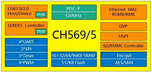
But more applications featuring RISC-V architecture are coming with, for instance, WCH CH569 RISC-V processor featuring USB 3.0, Gigabit Ethernet, DVP camera, and 1.25 SERDES block all managed by a RISC-V core clocked at 120 MHz.
CH569 (and CH565) processor key features and specifications:
- CPU – RISC-V (RISC-V3A) core @ 120MHz with hardware multiplication and division, programmable interrupt controller, low-power two-stage pipeline
- Memory – 16KB 32-bit SRAM, 32/64/96KB configurable 128-bit SRAM
- Storage
- Internal – 448KB code flash, 32KB data flash
- External – SD/eMMC controller with single-wire, 4-wire, 8-wire data communication mode. Complies with eMMC card 4.4 and 4.5.1 specifications, and compatible with 5.0 specifications
- Networking – Gigabit Ethernet controller with RGMII and RMII PHY interfaces
- USB
- Super high-speed USB3.0 host/device PHY with OTG support
- High-speed USB 2.0 host/device PHY
- Other High-Speed Interfaces
- 8/16/32-bit High-speed parallel interface HSPI with built-in FIFO, DMA support for up to 3.8Gbps transfer rate
- SERDES PHY (e.g. for optical fiber) up to 1.25Gbps
- Camera – 8/10/12-bit Digital video interface (DVP) with YUV, RGB, or JPEG compressed data
- Other I/Os and peripherals
- 4x UART up to 6Mbps
- 2x SPI master/slave interface
- 4x PWM
- 49x GPIO, 8 can be set to level/edge interrupt
- Active parallel port with 8-bit data, 15-bit address bus
- 3x 26-bit timers with PWM modulation output support
- Built-in watchdog timer
- Security – AES/SM4 hash, SRAM/EMMC/HSPI peripheral interface data encryption and decryption
- Misc – Unique 64bit ID identification number (Chip ID)
- Package – QFN68, QFN40

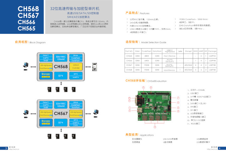
CH569 appears to be the first RISC-V processor part of WCH CH56x family of RISC (note: not V here) processor for networked storage applications with CH565, CH566, CH567, and CH568 offering a mix of Ethernet, SATA, USB 2.0, and other interfaces All chips come with the same 120 MHz RISC processor, and only 32KB RAM (128-bit wide), but the company claims the 128-bit DMA engine can transfer large amount of data.
What’s a bit confusing is that the first block diagram in the article looks to be for both CH569 and CH565, so one might think that all CH56x are based on the same RISC-V core @ 120 MHz, but others have reported that CH568 is based an on Andes NDS32 core. Typical applications for CH569 listed by the company include media streaming, network storage, ultra-high-speed USB3.0 FIFO, communication extension, security monitoring, and more.
At this point, there’s very little information available, and everything is in Chinese on the product page, but at least you can request more information and samples.
Via Claude Schwartz on Twitter.

Jean-Luc started CNX Software in 2010 as a part-time endeavor, before quitting his job as a software engineering manager, and starting to write daily news, and reviews full time later in 2011.
Support CNX Software! Donate via cryptocurrencies, become a Patron on Patreon, or purchase goods on Amazon or Aliexpress


Seems like a lot of nice hardware for (probably) pennies. I think you can bet on all the supplied code to drive those fast interfaces being complete garbage though.
This is unfortunately true, even two years after your comment. As of now, their BSP contains poorly documented code, half in Chinese, half in broken English. I am native Chinese speaker and I speak English good enough to do stand up comedies, and I don’t always get what they meant in their comments.
Some of the driver code is available only in BLOBs, aka .a files, while some are available in source code, both with ambiguous license terms. Many advanced peripherals have no register maps whatsoever, and the only way to use them is to use their BLOBs.
Even the CPU/RAM/ROM (!!!) don’t work as advertised. The CPU has an advertised 120MHz frequency, while in reality to use the full 448KB of ROM, you have to dumb it down to 96MHz, and it takes 8 CPU cycles to read the ROM, thus the necessity of a RAM cache. The cache is not even automatic — you have to explicitly relocate RAM code in both LD script and start.s.
The chip has 128KB+16KB of RAM, in which the 128KB DMA-able RAM is shared with ROM’s RAM cache, so even if all of your “fast” code can be compiled in to 64KB, it still eats half of your precious RAM. Making things even worse, there is no automatic CPU frequency dumb-down for ROM access. If you copy your fast routines to RAM, and set the CPU to run at 120MHz, when you jump to slow ROM code, the chip will crash.
So practically unless you change the calling convention and insert PLL adjustment code between function calls, you have to either live with 96MHz or less, or have 100% of your code fit within 96KB (max size of the ROM cache). Considering RV32 has a rather low code density, 96KB can do very little.
So all in all, despite having USB3, GMAC, DVP/HSPI, you pretty much have to choose to use only a small set of the chip’s advanced features before running out of RAM and ROM cache.
Just like everything else WCH has designed, CH569 was originally designed as an interface chip, and should be used as one. Anticipating this thing to be useful for anything more than just bridging interfaces would not be wise. If you anticipate this to be a cheaper alternate to Cypress FX3 or a more versatile FT600, then this could be great. If you anticipate this chip to be the only MCU in the system, well, just forget about it.
OpenPOWER never gets a mention, guess folk don’t like it.
” BlueGene/Q’s A2I POWER Core As Free and Open Source Silicon “
Is it a suitable core for a micro controller?
No I ment as open source, they quote 2.3 GHz @ .9w 45nm. Over at abopen . com
now under the Creative Commons Attribution 4.0 licence.
>they quote 2.3 GHz @ .9w 45nm
This article is talking about sub-ghz microcontrollers.. The reasons no one is making a noise about openpower in the sub-ghz parts that cost cents segment is that it’s totally unsuitable.
Most OpenPOWER processors are designed for HPC (e.g. supercomputer), so a bit out of topic here. The new A2I core might however be suitable for embedded SoC given the low power consumption.
A cheap Sigrok compatible logic analyzer based on this chip would be awesome.
YES, the HSPI is suit for communicate with FPGA/CPLD, USB2.0/3.0/Ethernet for communicate with PC, a nice choice for PC-FPGA interface