Lattice CrossLink-NX FPGA
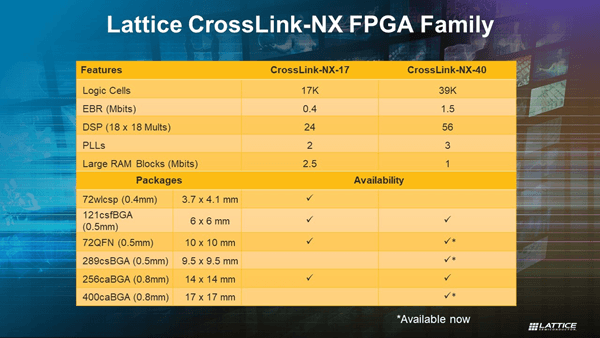
Lattice Semiconductor has announced the first product associated with its Nexus Platform, the CrossLink-NX FPGA designed for embedded vision and Edge AI applications. There are two offerings at this time, the CrossLink-NX FPGA 17, and the CrossLink-NX FPGA 40.

Recent Announcements
The Nexus Platform was introduced at the beginning of December 2019, and now CrossLink-NX has been developed and is being manufactured. The first announcements of Lattice Nexus Platform and The CrossLink-NX Product Family came as the company’s moved to capture the embedded vision systems market.
The Standout Features
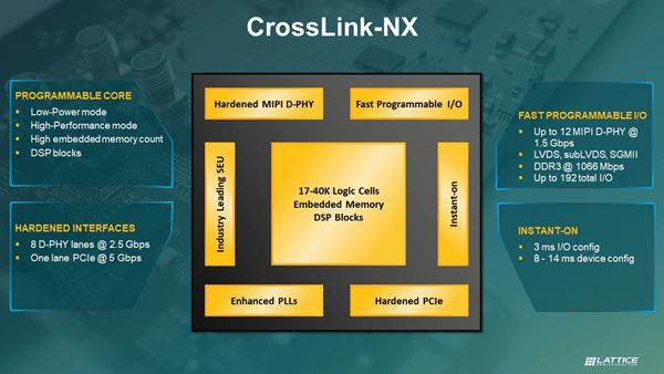
The low-power consumption, low soft error immunity, and 10Gbps MIPI are highlights of the CrossLink-NX FPGA. Other features include Instant On, with IO configured in 3 ms, and a total of 8 ms for the device.
The Cross-Platform FPGAs
The trends in technology are leading to devices that can cross function in a number of different tech environments. Nexus Platform systems are offered to support such applications as embedded vision, AI and IoT, video, hardware security and much more.
Architecture
Lattice has developed a proprietary FPGA architecture to optimizes DSP blocks and higher on-chip memory capacity, that foster higher performance in more power-efficient system infrastructure.
Edge AI
Edge AI processing is supported in order to expand into the embedded vision and automation sectors, by offering developers the processing ability for such functions as counting or presence detection.
There are two CrossLink-NX devices offered, the LIFCL-17 and LIFCL-40.
Possible Configurations
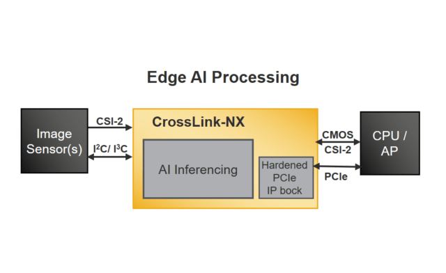
Edge AI Processing
- Bridge one or multiple CSI-2 image sensors to processor interface (PCIe, CMOS, CSI-2)
- Up to 3 Mb of internal RAM for processing
- Offloads inferencing from CPU for object detection/counting
- Combine video bridging and edge AI into a single device
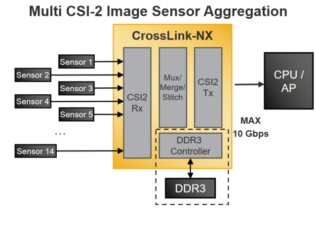
Sensor Aggregation
- Aggregate up to 13x MIPI CSI-2 image sensors into one MIPI CSI-2 output
- Stitch data together into a larger horizontal video frame
- Use external DDR memory to stitch data into a larger vertical video frame
- Arbitrate data from image sensors using unique virtual channel numbers
- Extend limited processor sensor interface capability and connect more sensors
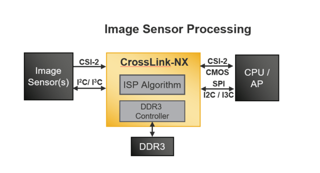
Image Sensor Processing
- Bridge one or multiple CSI-2 image sensors to processor interface (PCIe, CMOS, CSI-2)
- Integrate full functional universal video pipeline
- Examples: Debayer, color correction matrix, RGB gain, gamma correction…
- Offloads ISP functionality from the processor
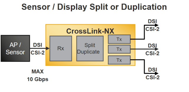
Signal Split or Duplication
- Split or duplicate input CSI-2/DSI signal to multiple video outputs (up to 14)
- Provide redundancy to sensor data in safety-critical applications
- Simplify applications which require one input to many display outputs
Visit the product page for more details.

Stephen started writing about technology after publishing sci-fi short stories. His first White-Paper, written in 2008, was well received and inspired him to continue writing about technology. Today he writes in the technology space full time, covering a multitude of topics. During the time he wrote part-time he edited hundreds of titles for large publishers, in science and technology. He lives in Staten Island, with his wife and children.
Support CNX Software! Donate via cryptocurrencies, become a Patron on Patreon, or purchase goods on Amazon or Aliexpress





We may get open source workflow support through Project Oxide (https://github.com/daveshah1/prjoxide).
Oxide would be great
One of the features is up to two hard “RISC-V compliant ALU”s. They’re only 32-bit, but it’s an interesting sign of how popular RV softcores have become.
“low soft error immunity” Huh?