Once upon a time Intel manufactured mobile processors for smartphones and tablets, but they eventually gave up as their solutions failed to gain traction. However, it looks like they may be back, as one customers required them to developer a chip with higher performance than Atom processors combined with a 2 mW standby power state.
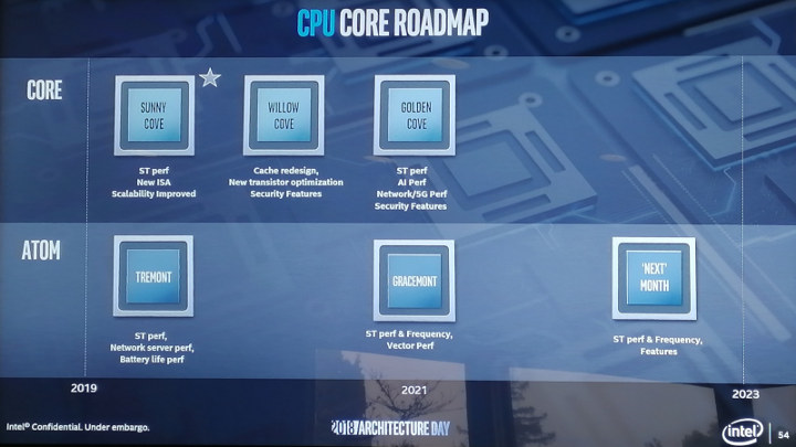
The chip was developed using “Foveros” 3D stacking technology was showcased at Intel’s Architecture Day 2018, but before going into further details, let’s have a look at Atom and Core processors roadmap to 2023 unveiled at the event.
First, Intel will have developed three new Atom micro-architectures going into 2023. As we’ve seen previously, Tremont will succeed Goldmont Plus microarchitecture found in Gemini Lake and Denverton processors, and improve single-threaded performance, network server performance, and battery life starting in 2019. Around 2021, Gracemont will be launched with again higher single-thread performance and frequency, as well as improvement to vector performance, and two years later (2023), the yet-to-be-named “Next Mont” will bring further single-thread performance and new features.
The top row of the roadmap reveals Intel Core processor roadmap with Sunny Cove, Willow Cove and Golden cove micro-architectures that will be updated year-on-year instead of every two years for the Atom family. What’s interesting here is that Intel has somewhat followed Arm’s big.LITTLE / DynamIQ by combining a “big” Sunny Cove processor with four “small” Atom cores in their Hybrid “Foveros” chip.
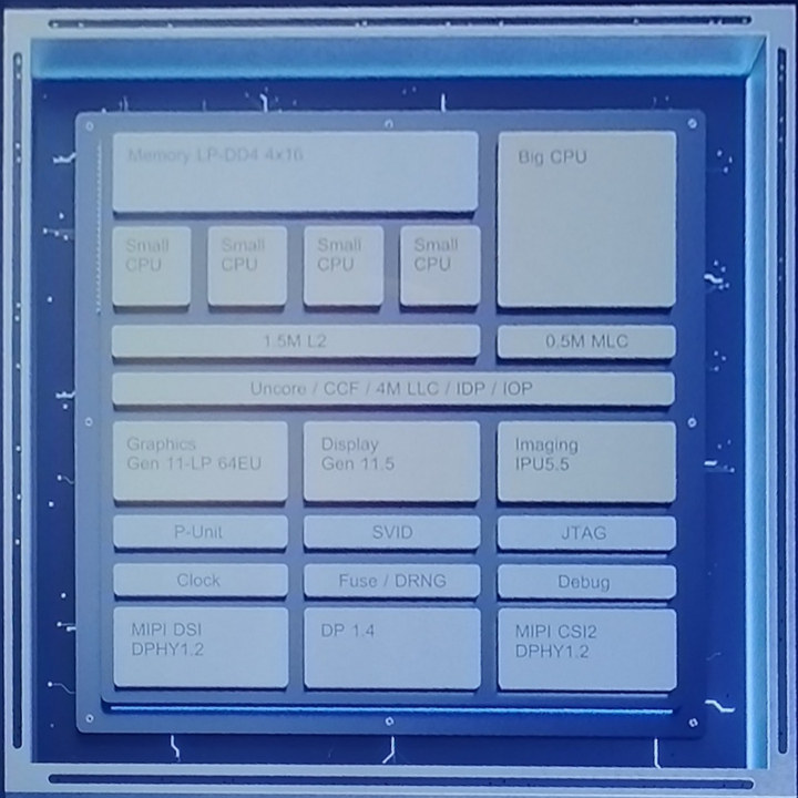
The big core comes with 0.5MB of private medium level cache, while the four small Atom (Tremont?) cores share 1.5MB of L2 cache. The chip further adds 4MB of last level cache, a memory controller with support for LPDDR4, 64 EU Gen11 graphics (yes, Intel also unveiled a new GPU capable of handling 4GK/8K), a Gen 11.5 display controller, an IPU 5.5 image engine, MIPI DSI and CSI interfaces, DisplayPort 1.4, and more. Foveros technology enables the integration of all those features into a tiny 12x12mm package with a 7W TDP, and 2mW standby power consumption.
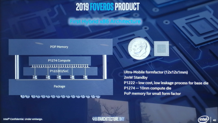
The P1274 compute die combining both Sunny Cove and Atom cores is manufactured using a 10nm process, while the P1222 IO chip is made with 22FFL process specifically designed for low power IoT and mobile products.
Intel did not disclosed the name of the customer, or the exact purpose of the chip, but as Anandtech points out the chip certainly targets mobile devices due to the power budget and tiny package, as well as support for features such as UFS storage and M.2 PCIe SSDs. The development board showcased at the event – and pictured below – also had a few SIM card slots.
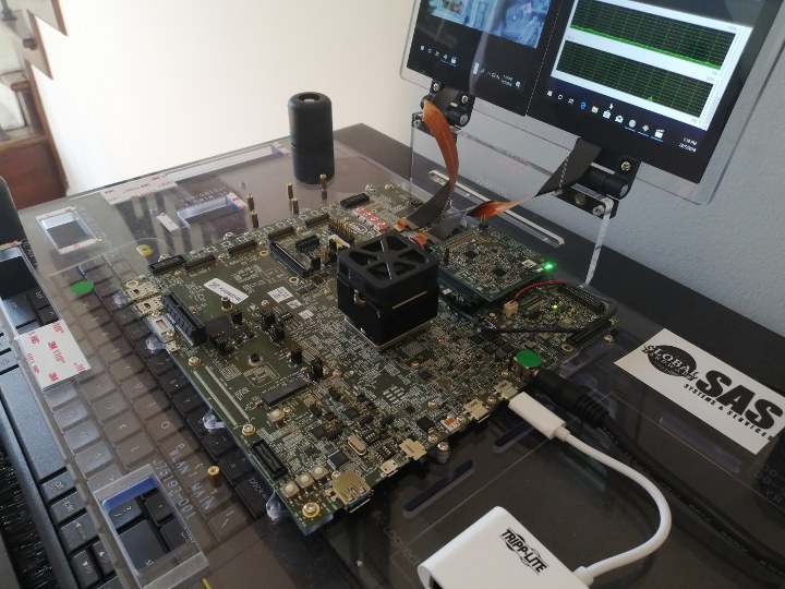
The 7W power budget is likely too high for smartphones, so I suspect Intel’s customer may want to compete against Arm laptops (aka always-on always connected mobile PCs) that offer over 20 hours of battery life on a charge. The new chip may be able to offer similar battery life, while delivering much better single thread performance thanks to the Sunny Cove core.
It’s unclear when the new hybrid x86 processor will be found into products, but Intel says it will be available to other OEMs too, and more Foveros Hybrid processors will be launched in 2019 and 2020.
Thanks to TLS for the tip.

Jean-Luc started CNX Software in 2010 as a part-time endeavor, before quitting his job as a software engineering manager, and starting to write daily news, and reviews full time later in 2011.
Support CNX Software! Donate via cryptocurrencies, become a Patron on Patreon, or purchase goods on Amazon or Aliexpress





That’s a large heatsink and fan!
It may be a very good move from them. Right now their processors are either low-power and low performance, or high performance and high power. The vast majority of workloads are still bounded by single-threaded performance, and having even a single high-performance core may be sufficient to make an atom perform as well as a core-i7 on a lot of programs. Also, operating systems have evolved a lot and their schedulers have been optimized for big.little architectures, so the benefits could be perceived without having to wait several years for operating systems to adapt.
>their schedulers have been optimized for big.little
Support for big.little seems patchy at best in mainline linux. I think last time I actually enabled the big.little scheduler on my odroid xu4 it caused the kernel to dead lock on boot.
Interesting there are 4 down votes but not one comment about how it works and it’s actually amazing. :p
You shouldn’t worry about down votes, I’ve always suspected that some visitors randomly click given that often informative responses are down voted (except for Jerry of course). Or maybe some fanboys just vote you down when you approach their fetish projects and don’t say exactly what they’d like to read.
I don’t really mind about down votes in general but with something like this if someone knows better then they would spend the extra 10s to write “actually, it works via blah, you need to enable CONFIG_BLAH and you’re set”.
Otherwise it just looks like what you said. Fanboys getting annoyed that someone dares say something they don’t like.
All I can see is CONFIG_ARM_BIG_LITTLE_CPUFREQ with a cpufreq driver and CONFIG_ARM_BIG_LITTLE_CPUIDLE with a cpuidle driver. I don’t know the specifics though.
Looking at the timelines and comparing with the ARM offering, i get the feeling that this will be a bit late to the game?
> this will be a bit late to the game?
Microsoft just recently made Windows’ scheduler fit for big.LITTLE…
With their generational fabnode advantage dissolved, Intel need a way forward. In this regard late is better than never.
Intel stuck at 10nm, AMD now on 7nm, even Amlogic S905x2 is 12nm. Next real speed boost needs low power high speed memory or low power high speed ssd, for portables.
> Amlogic S905x2 is 12nm
https://browser.geekbench.com/v4/cpu/search?utf8=✓&q=A95X is sufficient to get that S905X2 is clocked at ~1760 MHz max. If Amlogic needs a more expensive 12nm process for this then kudos to their competitors who manage to get their 28nm Cortex A53 clocked at 1800 MHz. The whole idea to switch to a more expensive process for absolutely no reason other than increasing manufacturing costs in a market where consumers only buy ‘as cheap as possible’ and energy consumption isn’t relevant seems brilliant! 😉
Surprisingly enough, next sweet-spot fabnote might be 22nm planar: https://semiengineering.com/foundries-prepare-for-battle-at-22nm/
The cost differences of 28nm vs. 14nm/16nm is really interesting. Especially for those people believing into fairy tales like dirt cheap TV box SoCs being done in a 12nm process. 🙂
Yep. The cost of designing devices on advanced nodes is rising exponentially with the nodes. Just like with many other things in reality, things are getting exponentially harder past a certain point, and we are well past it here — Intel can attest.
Many of us probably remember that it was expected to be impossible to go lower than 45nm many years ago. But extreme UV and electron beams have made details thinner and we’re now seeing 5nm on some products roadmaps. At least we know there is a wall : a transistor gate will always need to be at least 0.21nm wide as long as we use silicon 😉 The reliability may suffer from lower process nodes, thinking that each single atom becomes important to drive a signal is scary!
Honest question: Is GF or TSMC 7nm actually any better than Intel’s 10nm process except for the smaller number in the branding?
Quick googling shows otherwise:
https://wccftech.com/analysis-about-intels-10nm-process/
GF doesn’t have 7nm and won’t for a very long time, as they postponed their 7nm development.
Intel’s 10nm is broken, so yes, TSMC’s 7nm is a lot better, as it’s already shipping in working products, whereas Intel’s 10nm is shipping in some very poor Celeron processors only. Apparently they expect to have their 10nm stuff sorted by the end of 2019. Intel is also working on 7nm, using a different technology approach to their 10nm process.
I would take anything from wccftech with a a fistful of salt. That said, everyone measures their manufacturing process differently, so they’re no longer comparable one to one, as they use quite different technology.
For example, if you want to make RF products, the hot tech is gallium nitride, which isn’t used in normal semiconductors. It’s also being used in cutting edge FETs and some other niche technologies.
I wouldn’t take anything from wccftech, period. They’re the equivalent of monkeys on kbds in the IT news sphere.
>GF doesn’t have 7nm and won’t for a very long time
I think I actually meant Samsung.
>TSMC’s 7nm is a lot better, as it’s already shipping in working products,
TSMC’s 7nm process seems to be shipping parts that are clocking at ~2.5GHz (Apple A12). Intel’s current process is shipping parts that run at 5GHz. If Intel actually gets their 10nm working and shipping 5GHz parts does that mean they have the lead even though their branding is 3 digits off?
>I would take anything from wccftech with a a fistful of salt.
Other sites have similar metrics that don’t show a massive difference in the technical specs of Intel’s 10nm process and other’s 7nm process. For example:
https://www.semiwiki.com/forum/content/7602-semicon-west-intel-10nm-gf-7nm-update.html
Granted actually shipping working parts is a real world difference opposed to something that’s purely on paper.
As far as I can tell if Intel’s process was shipping working parts in volume they’d had something that is at least parity with TSMC and those parts would be running at much higher frequencies.
>That said, everyone measures their manufacturing process differently,
>so they’re no longer comparable one to one, as they use quite different technology.
That’s the point I was making. If we know that the node size is purely branding why does anyone use it for comparison.
> As far as I can tell if Intel’s process was shipping working parts in volume they’d had something that is at least parity with TSMC and those parts would be running at much higher frequencies.
As far as I know the only 10nm CPU Intel has shipped is the i3-8121U and that poor baby is running at a turbo of 3.2 GHz, much lower than 14nm CPUs. And that’s with a TDP of 15W.
Also TSMC 7nm SoC have CPU running at more than 2.8 GHz in Snapdragon 855.
Intel 10nm isn’t delivering years after it should have been in production, while TSMC has some high volume SoCs in production at 7nm. I’m confident Intel will recover with their next process, but at the moment they are lagging behind.
Intel’s answer has been to throw heat at the fast CPU problem but sub 12 nm is not as forgiving due to area vs heat removal. Hence power sipping designs gain advantage.
>Intel’s answer has been to throw heat at the fast CPU problem
Do you honestly think their design teams think like that?
>As far as I know the only 10nm CPU Intel has shipped is the i3-8121U
That’s true for right now but the reports (not saying they have any relation to reality) say they expect to have this working in the new year.
>Also TSMC 7nm SoC have CPU running at more than 2.8 GHz in Snapdragon 855.
Doesn’t seem to actually be shipping yet and only one core runs at 2.8GHz.
>I’m confident Intel will recover with their next process,
Maybe. It might not even matter if iPhone sales don’t improve and the only pressure on TSMC from Apple is to lower costs. There isn’t much point in spending yet more money on new processes if Apple isn’t willing to pay for it.
This seems like a much better attempt at getting into the less bruteforce parts of the market. The previous attempt with Atom for mobile and the Quark stuff for “IoT” was a mess.
If they can actually get this stuff into consumer mobile devices it’s possible we’ll have some devices that can run a mainline kernel without losing the GPU and have video encoder/decoders with decent drivers etc.
Where will you fit the big heatsink and fan on your pocket IOT battery device?
That photo is probably not of one of the IoT targeted chips.. and why would I need to think about where the cooling goes? That would be for the people designing the hardware to worry about. Do you have weird issues with Intel like Blu? Did Intel sleep with your wife too?
Name calling from a alleged adult!
ugh, what name calling? who said anyone was “an adult”? but anyhow I’m taking that as a yes and a sign that a rational discussion isn’t going to be forthcoming. I’m sure those bad guys at Intel really hurt you but if you want to be angry at anyone be angry at the DRAM vendors that are fleecing all of us regardless of what brand we fanboy for.
I am sure that the client for this Foveros chip is Microsoft, and that it would be utilized in its upcoming “Centaurus” two-screen foldable small tablet (which would also function as a small laptop).
(That’s like the rumored Andromeda device, but bigger).
It could also be Google, with Microsoft keen to fight back against Windows on Arm and Chromebooks on Arm, they may want Google to get ChromeOS on Intel back in the game?