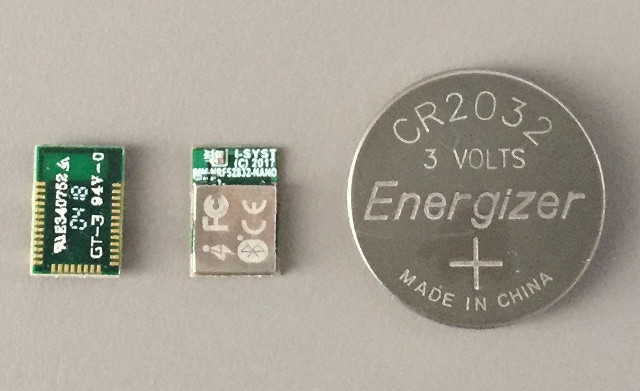
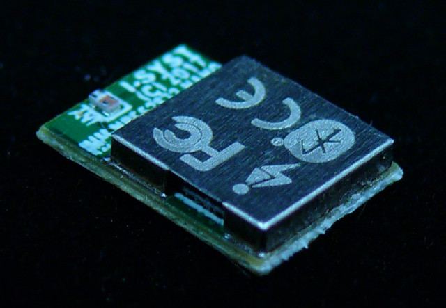
If you have a project requiring a programmable Bluetooth 4.x/5 module that’s as small as possible, Canada based I-Syst may have what you need with their IMM-NRF52832-NANO module measuring just 10 x 7 x 1.6 mm.
The module is based on Nordic Semi nRF52832 Arm Cortex-M4F SoC with Bluetooth 5 LE (no long range support) and ANT+ connectivity, and exposes up to 30 I/Os for your project.
- SoC – Nordic Semi nRF52832 32 bits Arm Cortex-M4F @ 64MHz with 512KB Flash, 64KB SRAM, 2.4GHz multi-protocol transceiver
- Connectivity – Bluetooth 5 LE, ANT+, Type 2 NFC -A Tag with wakeup on field
- Up to 30x I/Os:
- 3x SPI Master/Slave
- 2x 2-wire Master (I2C compatible)
- UART (CTS/RTS)
- 3x 4 channel PWM
- 8x configurable 12 bits, 200 ksps ADC
- Digital microphone interface
- Quadrature decoder input
- Sensors – Temperature sensor
- Security – AES HW encryption
- Misc – 32MHz & 32.768KHz crystals, low power comparator
- Power Supply – 1.8V to 3.6V DC input; DC/DC power mode inductors
- Dimension – 10 x 7 x 1.6 mm
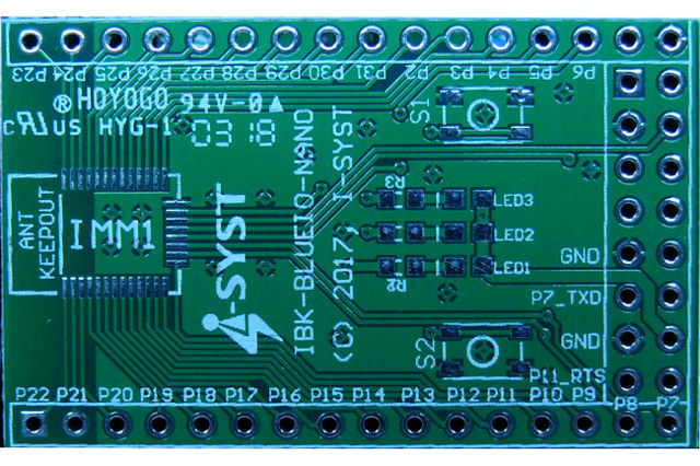
The module can be used without extra components and “the only space required on your PCB is the module size itself”, which makes it ideal for wearable and space-constrained applications. A getting started guide, source code samples, including iOS & Android apps can be found on the developer’s blog. A breakout board – pictured below – can also be provided to speed up development or for evaluation.
 IMM-NRF52832-NANO miniature module is sold for $18 on Tindie plus shipping, but you may also consider spending $3 extra for the DIP32 breakout board. More documentation can also be found on the Tindie link.

Jean-Luc started CNX Software in 2010 as a part-time endeavor, before quitting his job as a software engineering manager, and starting to write daily news, and reviews full time later in 2011.
Support CNX Software! Donate via cryptocurrencies, become a Patron on Patreon, or purchase goods on Amazon or Aliexpress


That’s an impressive amount of I/O for such a small board. In my opinion there is one mistake with the breakout board : it should have been one row longer so that Vcc and GND are exposed on the top and bottom rows, making it breadboard-friendly. Here it will require soldering a dual-row connector on the top in order to use the pins on the right, which possibly is acceptable to the users who want to expose all I/O, but those who don’t will still have to do it just for the power. It’s no big deal though.
It could possibly replace some microcontrollers or even ESP32/8266 boards in certain projects.
Oh yes, replace esp8266.. with 18$
Can I make a suggestion for board designers? Please stop putting these board horizontal. That covers up all the holes on the breadboard and makes using them unplesant. Please put a 2x.1″ header along the bottom (so devices with antennas can be pointed *up* away from the board. Two rows of bent 1x headers go on to the two sets of pins at the bottom–one on each side. That way the board can plug into the inner 0.3″ row of holes on the breadboard and leave a lot of room for connections.
USB or debugging connectors can easily go on the sides.