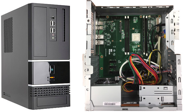
GIGABYTE, Socionext and Linaro have partnered to design a software development platform compliant with 96Boards Enterprise specifications, with GIGABYTE taking care of manufacturing the hardware based on Socionext SC2A11 processor, while Linaro will provide support via 96Boards community.

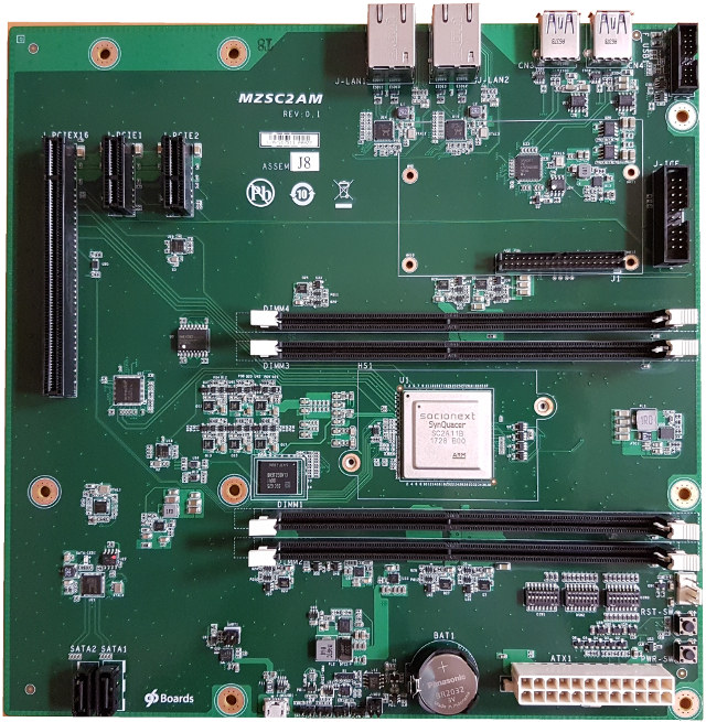
GIGABYTE SynQuacer platform preliminary specifications (based on photos and SC2A11 specifications):
- SoC – Socionext SynQuacer SC2A11 24x ARM Cortex-A53 MPCore cores @ up to 1GHz, with 32KB/32KB I/D L1 cache, 256 KB L2 cache, and 4MB L3 cache (5W power consumption)
- System Memory – 4x DIMM slots for 64-bit DDR4-2133Mbps with ECC up to 64GB
- Storage – 32GB Samsung KLMBG2JENB-B041 eMMC 5.1 flash + 2x SATA interfaces
- Connectivity – 2x Gigabit Ethernet (RJ45) with IPSec Network Offload Engine
- USB – 2x USB 3.0 ports on motherboard (via Renesas D720201), 4x USB ports on front panel via expansion board
- Audio – 1x microphone input, 1x speaker output on front panel
- Expansion – 1x PCie x16 slot (limited to 4-lanes), 2x PCIe x4 slots, other headers for expansion and/or debugging
- Misc – Power button, power and activity LEDs, reset and power switches, configuration switches, RTC battery
- Power Supply – ATX connector + ATX power supply
- Dimensions – board: microATX board (96Board Enterprise compliant)
Linaro have been working on Socionex SC2A11 SoC using their PEC boards for a while, and if you want more details you may check out Linaro Connect Budapest 2017’s presentation. Multiple PEC boards can be interconnected offering up to 1536-core servers, with those systems suitable for IoT gateways, edge computing and servers running programs such as Hadoop/Spark, e-Commerce platforms, OpenStack, and so on. As of March 2017, Socionext SC2A11 supported ARM Trusted firmware, UEFI (edk2), Linux 4.5 with all drivers, Centos 7 Aarch64 rootfs, and Hadoop.

The new development platform should become available in December 2017, and a prototype will be demonstrated during Linaro Connect San Francisco next week on September 25-29, and Yasuo Nishiguchi (Socionext) will present a related keynote at the event.

Jean-Luc started CNX Software in 2010 as a part-time endeavor, before quitting his job as a software engineering manager, and starting to write daily news, and reviews full time later in 2011.
Support CNX Software! Donate via cryptocurrencies, become a Patron on Patreon, or purchase goods on Amazon or Aliexpress


I don’t understand the point of these Cortex-A53 10+ core designs. Kirin 960 or Exynos 8895 will run circles around this thing. The only workloads these will run more efficiently are completely theoretical and when you throw in total cost, it’s completely stacked against this. Samsung, Huawei, and Qualcomm are the only ones that stand a chance in the server market because they have the cash.
If they need to validate ARM SBBR, just take a chip from a phone and add some firmware magic on top. If you’re not building on 16nm or smaller, don’t bother taping out a chip because it’s kind of dead on arrival.
Why waste a high performance hierarchical NUMA interconnect design with slow in-order cores? It’s frustrating to see money being tossed in the trash.
@lvrp16
Putting aside distributed computing like Hadoop, half the cheap VPS requests at lowendtalk.com would be more than satisfied with an instance on this board.
It is still too expensive to compete against x86 let alone cell phone chips for VPS. 24 x 1GHz is half the performance of one Ryzen 4-core die. The energy savings is moot when the rest of the stuff exceeds the power consumption by several folds.
If they arent building off an ARM architectural license, it is basically a wasted effort and they will go the way of Calxeda.
Designs like this have the flaw they tell the customer what the customer wants, when no one really knows.
Arm and MIPS ( Imagination has sold its MIPS CPU business to California based Tallwood ) need to agree on a free opensource plug in CPU socket. So as to encourage the market adoption and customer purchase. INMHO
The rest of Imagination technologies is being bought by Canyon Bridge Capital Partners for £550m. ( part China funded )
MIPS was sold at a loss, MIPS CPU business to California-based venture capital firm Tallwood for $65m (£48.2m), making a loss on its original investment of $100m.
This isn’t as bad as it looks. 24 of these cores will not perform that differently than 8 core Avoton and should be considerably faster than the 4 core version. That said, there will be need to not rely on bad web servers like Apache for this.
@lvrp16
@theguyuk
You’re both forgetting this is a development box meant for customers to sample and profile their use-cases before scaling it with a production server up to 512cores. Check out: https://www.youtube.com/watch?v=nhPm7d59t8c
Hadoop, mining cryptocurrency, AI, compile server, and VPS are all possible workloads.
> MIPS was sold at a loss
Hard to say. ImgTec is PowerVR, MIPS and Ensigma. They could have transferred certain IPs from MIPS to their other divisions before selling or they might have made up for the $40m margin in preexisting royalties over the last couple of years. It’s sorta like how people only buy Windows for Office and games. Take the package apart and it’s pure speculation on how well each part will fair in the market on their own.
@cnxsoft
isn’t it mini-itx rather than micro-atx ?
@lvrp16
Why theoretical? There are plenty of present workloads that could make good use of 24 cores. Whether this particular SoC is a good candidate for some of those workloads – that’s part of the reason this devboard exists.
@nobe
Board is u-ATX. m-ITX has a single PCIe slot.
So … what will the price be of this motherboard with 24core CPU? 100 USD? 200 USD? 70 USD?
@lvrp16
Don’t forget that this is just a nice easy to use R&D/dev system for a processor that is designed to be combined with a proprietary switch. The result is a cpu solution that one day is aimed to scale to 64 CPUs/1536 cores.
http://www.socionext.com/en/download/catalog/AD04-00121-1E.pdf
@Sander
I would only be interested in the price tags of the so called PEC (Processor Element Card with the 24 core SC2A11 SoC on it) and the SBB (System Bridge Board — the one with 9 PCIe ‘channels’ using the SC2A20 ‘SoC switch’ to interconnect 8 PECs) since I don’t think there exists a single use case where this ‘SynQuacer’ could shine.
That being said I find such an evaluation system as the above consisting only of one SC2A11 a bit… weird? I would be interested in how well the Socionext attempt to cluster up to 64 such SC2A11 equipped PEC using PCIe 2.x interconnects really works so an evaluation system should consists of one SC2A20 and at least 2 x SC2A11.
I also fail to understand the numbers shown on the slides from Linaro connect (eg. talking about a ‘Chip Interconnect Bandwidth’ of 5 GB/s compared to 38.4GB/s for the Intel system. If it’s PCIe 2.x we’re talking about 5GT/s per lane, 8b10 encoding and therefore with a x4 setup about 2GB/s: 500MB/s * 4)
with PCIe 2.x is misleading due to 8b10b encoding and 5Gbps meaning 400MB/s in reality)
So it’s like one xeon broken up into 24 atom class cores for oodles of money. I’m seeing only 2 or 3 customers with tons of venture money to throw on the fire before going bust in this chips future.
@blu
Sure there are plenty of workloads, the problem is that each individual task running on a core will be limited by the performance of a 1GHz A53 which is abysmal. We’re speaking about the lowest possibly frequency we’ve seen over the last 5 years coupled with a low-end CPU core. I suspect that a single Armada8040 CPU (4xA72 at 2 GHz) could already beat it, and at the same time ensure faster completion each time there are less than 24 tasks to run in parallel.
The only possible benefit of using a 1 GHz A53 is power efficiency which is much better than A72 or any xeon (and possibly atom). It will definitely count if you need to scale to 1536 cores since the total rack power draw might be lower with the A53 than with better chips for the same total performance.
@willy
Power efficiency is indeed the key here – once a task is matched to the parameters of the hw, you scale that by the TDP and see if you’re at a gain when you deploy across a multitude of such hw, vs using something larger. But I would not write off that SoC so quickly — after all it’s 24GHz of reasonably-good IPC at the cost of 5W. It’s a matter a finding a good task match (not necessary a solvable problem).
Looking at the params of the SoC, what bothers me the most is the cache setup.
@blu
No it’s not 24 GHz of good IPC, it’s 24x 1GHz of moderately acceptable IPC. In terms of latency it will really not be good compared to many other solutions. Also you need to keep in mind that the memory and I/O bandwidths will be shared between all these cores, which doesn’t help much either. But sure, it’s possible to find *certain* workloads for which it’s not a problem at all.
Performance discussion aside, one of the positive outcomes here is that we may see some additional uptake of ARM in the development community. This system bridges the gap between the cheap, but resource limited SBC’s we are all used to, and the expensive enterprise grade ARM platforms (Cavium, APM, etc.) that individuals don’t purchase. Of course, the price for this system will need to be reasonable in order to gain any traction.
@willy
Whether we call it ‘reasonably-good’ or ‘moderately-acceptable’ is irrelevant – A53 is the best in-order 64-bit uarch there’s today, with avaliability in volumes. As re 1x 24GHz vs 24x 1GHz – the whole point in finding a good-match task for the platform is one which scales linearly with the cores. Ergo, a good-match task would be equal to 24GHz sequantial performance.
Yet a few more details on Charbax videos: max memory 64GB, the 16-lane PCIe slot is actually limited to 4 lanes, and it will really be a single Gigabit Ethernet port eventually.
https://www.youtube.com/watch?v=kIwop47HDtw&feature=youtu.be&a=
The thing that makes 1GHz Cortex-A53 systems (like a Raspberry Pi, for example) low-performance is absolutely the limited memory bandwidth and size available on a single-channel 16-bit DDR3 interface meant for a low-end settop, or even high-end mobile phone applications, and the poor storage potential of the low-cost flash that microSD cards use and primary storage on eMMC provides.
Give a Cortex-A53, even just four of them, a reasonable /amount/ of RAM, and a SATA SSD (or NVMe..) and the performance is pretty spectacular in comparison to your average mobile SoC. All you’ve got to do is take away the latency of the lower end storage. This Socionext chip does this with L3 cache (that helps a lot), too, along with the multi-channel, 64-bit DDR interface and the ability to host disks that can do 500MB/s (and actually get to that data rate).
There are always people who are going to spend all their time talking about IPC and comparing to the $2500 latest Xeon processor with 16+ cores and whatever AMD are hawking this week at a $1200 price point, whining about the number of lanes on PCIe, the number of RAMs, the number of clocks per second, and the reality is that holistically unless you are trying to run the latest 4K UHD gaming masterpiece on 3 monitors you’ll never notice the difference between x16 and x4 PCIe graphics, or the ‘low’ core clock rate because you can get genie effects and transparency and smooth desktop usage you’d want – again considering this is not a gaming rig or a targeted benchmark platform – on, say, a 1GHz Cortex-A8 with an Adreno 200. Or a 400MHz PowerPC 603e with 256MB RAM (hi blu!)
Part of the problem with Arm systems right now is nobody is optimizing software for them except for the Android use case, and that Android software is not the same stuff you’ll get on a server-class system. There are no AArch64 code paths in pixman, for example, or Mesa, or for LZO or gzip (I do not mean doing a memory copy using the vector register file.. I mean real optimization), use of Advanced SIMD is really limited to something like encryption using the new AES/SHA instruction sets. 60% of every Arm processor you can find on these dev boards, the performance is dumped on the floor because the only performance they really needed on a cellphone is something to throw GPU command lists around, and the software to do exactly that. Projects like Firefox and Chrome (and V8 et al.) don’t get the AArch64 optimizations they could have because nobody has a development system that’s not basically a phone with the case hacked off, and they can’t appropriately test the results for a release.
This box changes that. You’ll see improvements, like we saw improvements going from softfloat to hardfloat on 32-bit ARM, or actually using AltiVec on PowerPC back in the day, or even running a real 64-bit stack on a Raspberry Pi instead of being locked in to an armv6-optimized 32-bit Linux distribution.
@meows
I more or less agree with you, but there are only two questions remaining on this: (1) when this will be available and (2) what’s the final price will be.
@meows
Hey Neko. I too think the A53 is largely underestimated by the general populace – A53’s IPC in well-optimized scenarios is perfectly fine for everyday use — about ~2-2.5 times worse than the IPC of much larger-area desktop chips for general-purpose applications. Which, considering the power envelope of the A53, is nothing short of great. It’s usually everything else in the SoC (and around) that drags the A53(s) down. And yes, memory channels are a major factor there. A typical example can be seen in tests like GEMM, which are essentially exercises in prefetch/BW utilisation — there A53 performs well, until data overruns the cache hierarchy – then the A53 tanks (https://github.com/blu/gemm#results)
Shipping moved to January 2018.
Reservations are up @ http://sp.chip1stop.com/socionext/
So it looks like this “sub-$1000” box becomes over $1000 box. Looks like it’s shipping for $1250 in basic configuration. Hmm…