Intel had their annual Investor meeting day on the 10th of May 2012 in Santa Clara where we would learn a few things about what’s ahead for Intel and the semiconductor industry.
Paul Otellini, Intel President and Chief Executive Officer, started the meeting by giving some numbers about Intel results and showing opportunities existing for cloud and data center, personal computing, mobile devices and intelligent systems (for automotive, retail and communications markets). One interesting point was the tremendous growth in data Intel expects from 2,500 Exabytes per year (7 EB/day) today to 8,000 Exabytes by 2015 which the majority of the growth lead by Big data. He also boasted about Intel technology advantage. For example, Intel introduced High-K Metal Gate technology in 2007 and competitor only got it in products last year (btw Samsung Exynos 5 uses HKMG). They recently introduced Tri-gate technology and they only expect competitors to catch up within 4 years. Finally one of the slide (see below) shows that Intel intends to be able to manufacture silicon using 10 to 5nm technology sometimes after 2015.

The technology to achieve this feat is still at the fundamental research stage however.
You can read the presentation (PDF) for more details.
Kirk Skaugen, General Manager of the PC Client Group, mainly talked about Ultrabooks which are high-performance, expensive (700 USD up) and thin notebooks. Intel Haswell Processor is designed to power Ultrabooks (in 2013) able to get 10 days of connected standby providing 20 times more efficiency than Intel iCore 5 device available in 2011. If you want to know more about the future for Intel based PC, Laptop and Ultrabook, you can read the presentation.
Diane Bryant, Vice President & General Manager of the Datacenter & Connected Systems Group, mainly talked about high end servers, but there is also a small section about microservers showing Xeon processors (Ivy Brigde) consuming 17W and the lower-end Atom Centerton SoC consuming a mere 6W. You can download the PDF presentation to know more about Intel datacenter and cloud solutions, customers and prospects.
Now let’s move to smartphones and tablets with Hermann Eul & Mike Bell of Intel Mobile and Communications Group. They started by showing Intel technological know-how for mobile applications and Intel R&D commitment with over 3,000 engineer working on software for Windows, Linux (Intel is No. 2 contributor) and other operating systems, including 1,200 working on Android for mobile.
Then they gave some details about Atom Medfield processor, their first smartphone processor, which can be integrated into smartphones that support 8MPixel camera, 1080p video via HDMI and last 14 days on a single battery charge (using a 1460mA battery). They also mentioned Anandtech article showing Medfield based Lava XOLO X900 beats the competition in terms of performance (for some benchmarks) and matches the power consumption of existing smartphones.
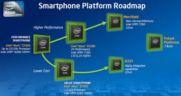
They also showed their smartphone platform roadmap with processors for both the high end and lower end segments of the market.

At the higher-end, we would get:
- Intel Atom Z2580 with Intel XMM 7160 LTE + 2X HSPA+ providing twice the performance of Medfield.
- Merrifield processor with XXM 7260 using 22nm manufacturing process.
and the lower-end:
- Intel Atom Z2000 @ 1GHZ with XMM 6265 (HSPA+)
- Intel Atom 6331 (22nm)
as well as future processors based on 14nm technology.
Intel also provided their tablet roadmap with Clover Trail 1.8 GHz 32nm processor (2012), Bay Trail 22nm processor (2013) and next generation processor (no name yet) using 14nm process (2014).
Have a look at the presentation for more information.
Brian Krzanich, Chief Operating Officer, gave a presentation about manufacturing and fabs which I would not normally mention in this blog, were it not for this slide:

Currently, silicon Fabs use 200mm wafers which requires company to generate 3 to 5 billions in revenue to stay afloat representing all companies in the chart above (Elpida recently filled for bankruptcy before being bought by Micron). Now some companies starts to move to 300mm. A manufacturing site designed for this type of wafer requires 9 to 12 billions in revenues (shown in green above), but as it scales it becomes much more cost effective than a 200mm wafer Fab. That means that companies such as Freescale, NXP Broadcom and AMD would eventually have to go Fabless to survive, be bought or go bankrupt. After 2015, Fabs designed for 450mm wafer will start to show up (I’m pretty sure there is a mistake on the slide above and “300mm Fab” should read “450mm Fab”). This type of Fab requires 15 billions in revenues according to Intel, which would means that only 2 or 3 companies in the world, namely Intel, Samsung and possibly TSMC will be large enough to have manufacturing sites, unless companies such as Texas Instruments and Toshiba buy smaller players in the meantime.
If you are interested, you can check the PDF.
There were also two other presentations by the sales team and the CFO. You can listen to the webcast and access all the presentation slides on Intel Corporation 2012 Investor Meeting Webcast.

Jean-Luc started CNX Software in 2010 as a part-time endeavor, before quitting his job as a software engineering manager, and starting to write daily news, and reviews full time later in 2011.
Support CNX Software! Donate via cryptocurrencies, become a Patron on Patreon, or purchase goods on Amazon or Aliexpress


