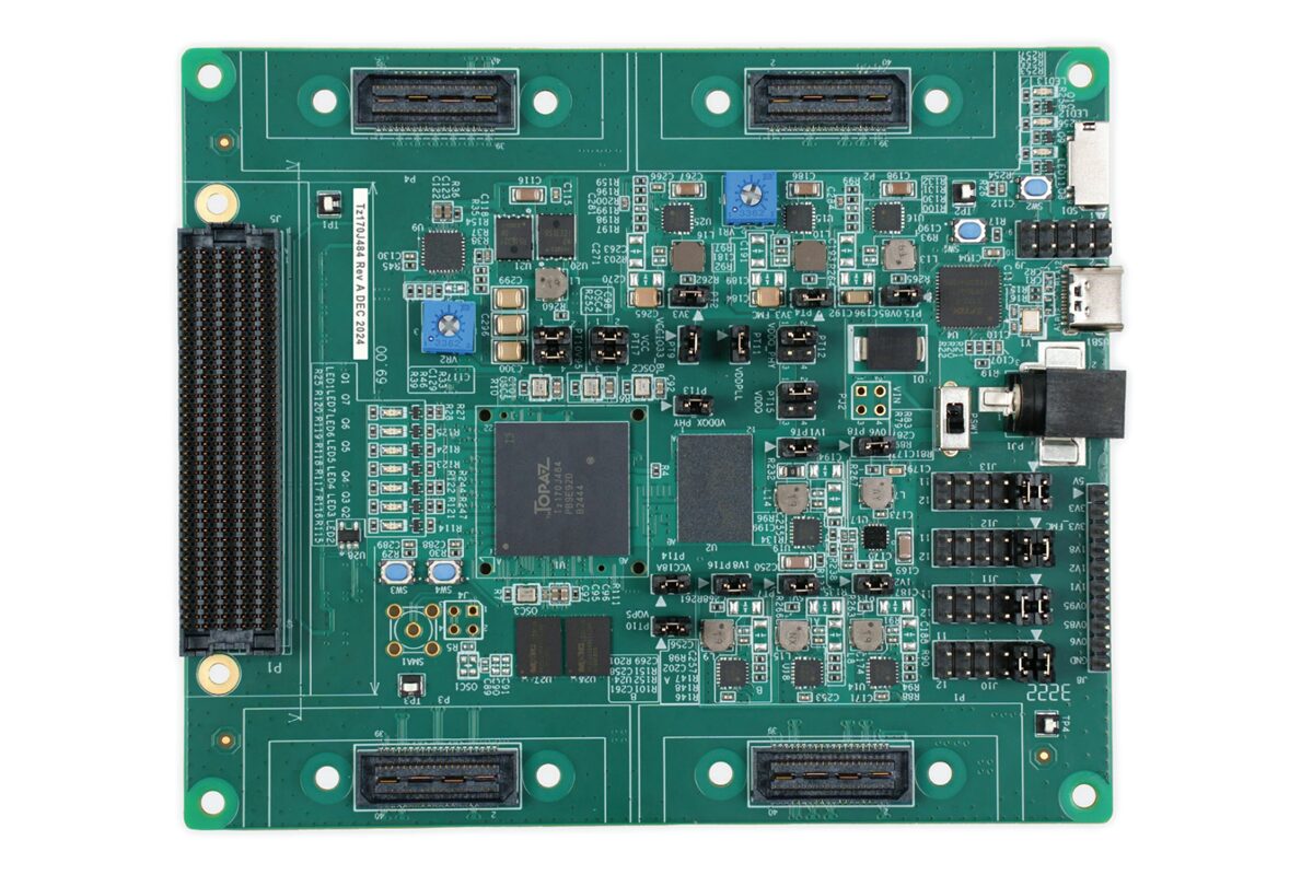
The Topaz Tz170b FPGA devkit from Efinix is a compact FPGA evaluation platform built around the Efinix Tz170 FPGA. This FPGA is built around a low-power, high-density 16 nm Quantum fabric and comes in a compact 484-ball FineLine BGA package. The company mentions that the board supports hardware-level MIPI D-PHY with data rates of up to 2 Gbps per lane and hardware-level LPDDR4 memory controller, making it ideal for high-speed embedded systems, vision processing, and custom SoC designs. Additionally, it includes 256 Mbit of LPDDR4 memory, dual SPI NOR flash memories, and high-speed QSE connectors for Efinix or custom daughter cards. Expansion is further enabled by a low-pin-count FMC connector, a microSD slot, user LEDs, and push buttons. Clock options include 33.33, 50, and 74.25 MHz oscillators, and a full range of onboard regulated power sources for stable operations. These features make this device useful for applications like edge AI, […]
TinyBeast FPGA – A Microchip PolarFire MPF300T/MPF100T FPGA PCIe reference design (Crowdfunding)
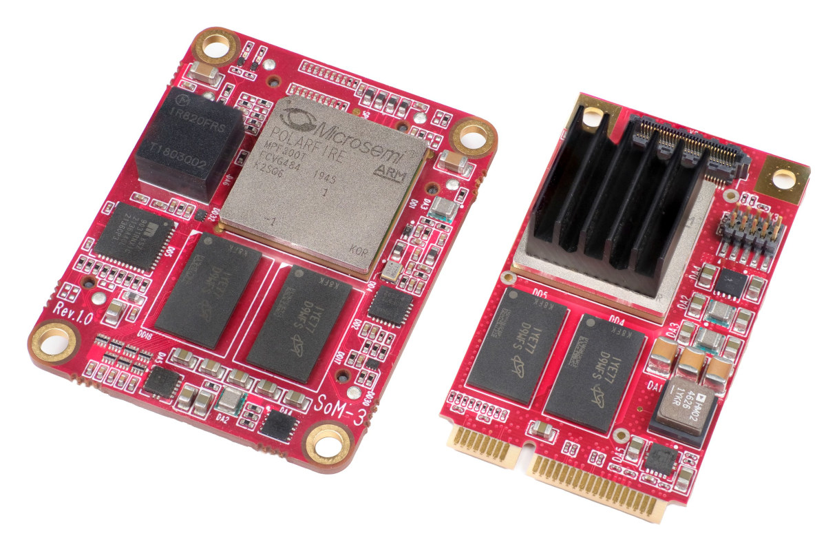
TinyBeast FPGA is a compact module based on Microchip PolarFire MPF100T or MPF300T FPGA with up to 300K logic elements and a hard PCIe interface that is suitable for automation, measurement, and robotics applications. Two versions of the module are available: the TinyBeast FPGA P mini PCIe module designed for integration with embedded systems, and the TinyBeast FPGA S with B2B connectors designed to be connected to a carrier board. TinyBeast FPGA P TinyBeast FPGA P specifications: FPGA – Microchip PolarFire FPGA TinyBest FPGA P-300 – MPF300T-1FCVG484E FPGA with 300K LE, 10.6 Mbit embedded RAM, 924 DSP blocks TinyBest FPGA P-100 – 100K LE, 5.2 Mbit embedded RAM, 288 DSP blocks System Memory – 4 GB DDR4 memory Storage – SPI flash Host interface – PCIe x1 Gen2 as EP via mini PCIe edge connector Expansion – Samtec SS4-30-3.00-L-D-K I/O connector for GPIOs and up to 12.7 Gbps transceivers Debugging […]
Sapphire Edge+ VPR-5050 “AMD Embedded+” mini-ITX motherboard combines AMD Ryzen V2748 CPU and Versal AI Edge VE2302 SoC FPGA
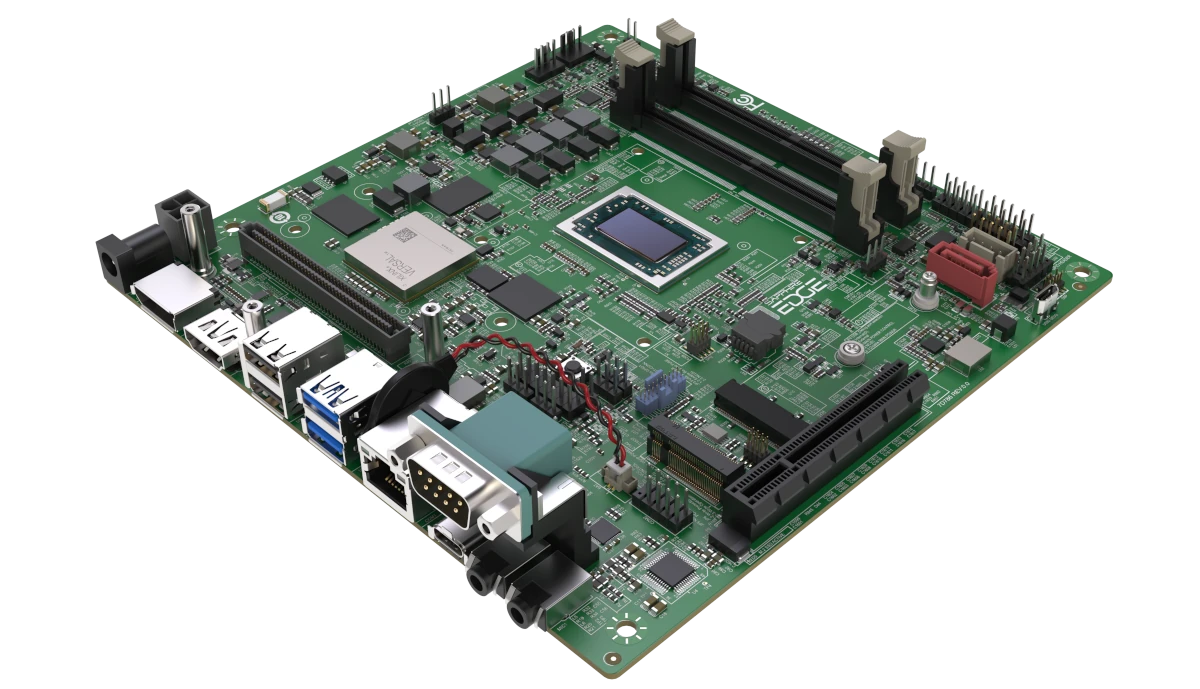
Right in time for Embedded World 2025, Sapphire Technology has introduced the Edge+ VPR-5050 “AMD Embedded+” mini-ITX motherboard with AMD Ryzen V2748 octa-core CPU, and AMD Versal AI Edge VE2302 adaptive SoC that combines Cortex-A72 hard core with FPGA fabric. It’s an update to last year’s VPR-4616-MB mini-ITX motherboard with the same Versal VE2302 adaptive SoC, but a lower end AMD Ryzen R2314 quad-core processor. Two versions of the Edge+ VPR-5050 are available: the VPR-5050-MB and VPR-5050A-MB with the only obvious difference from the specifications being a 64GB eMMC flash on the “A” model, and the different RAM capacities (2x 4GB LPDDR4 vs 2x 8GB LPDDR4). Sapphire Edge+ VPR-5050 specifications: AMD Embedded+ Architecture Adaptive SoC Subsystem Main IC – AMD Versal AI Edge VE2302 with dual Arm Cortex-A72 core processor @ up to 1.6 GHz, dual-core Arm Cortex-R5F, 23 TOPS AI engine, FPGA fabric, etc… System Memory VPR-5050-MB – 2x […]
Haasoscope Pro open-source, real-time sampling USB oscilloscope supports up to 2GHz bandwidth (Crowdfunding)
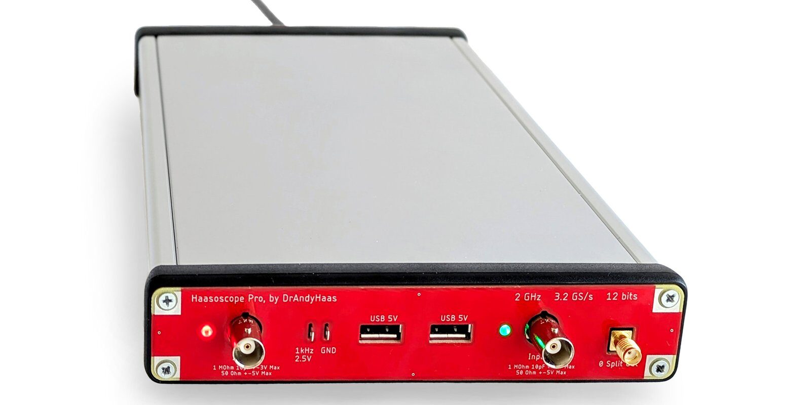
The Haasoscope Pro is an open-source hardware, high-bandwidth, and real-time sampling USB oscilloscope. Building upon its predecessor, the Haasoscope, the new Pro model offers a bandwidth of 2GHz, 12-bit resolution, and a 3.2GS/s sampling rate. The Haasoscope Pro USB oscilloscope is “designed to be low cost, while maintaining super-fast performance.” While it only comes with 2 channels, the flexible design makes it possible to combine and sync multiple devices (using Cat5 cables) to double the sample rate or add more channels. The oscilloscope works with standard x10 passive probes but a custom active probe, the Haasoscope Pro-be, is also offered. It supports the full 2GHz analog bandwidth and is priced much cheaper than similar probes. The Haasoscope Pro USB oscilloscope’s high sampling rate and bandwidth make it ideal for radio frequency signal analysis and high-speed digital debugging. It is similar to the ThunderScope Thunderbolt and PCIe oscilloscope which offers more […]
Vaaman reconfigurable edge computer features Rockchip RK3399 SoC and Efinix Trion T120 FPGA (Crowdfunding)
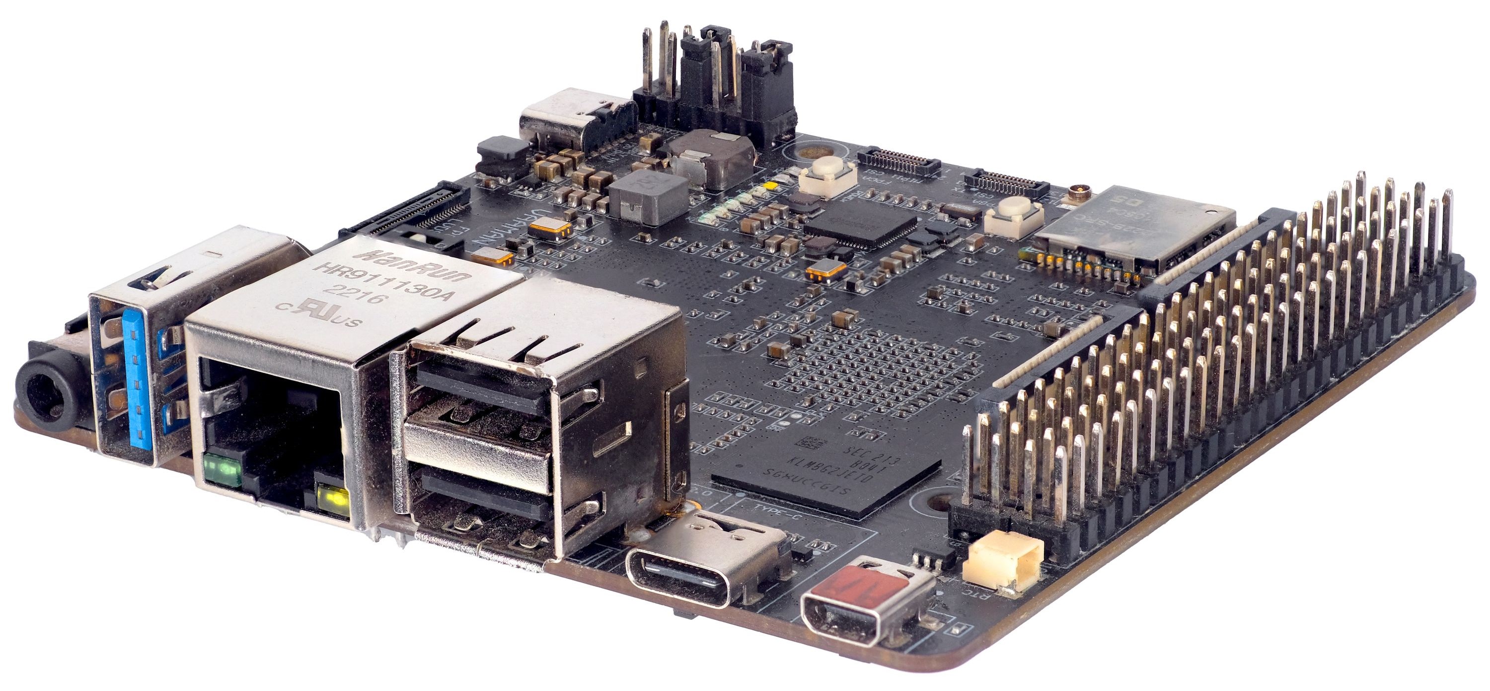
Vaaman is a reconfigurable single-board edge computer that integrates a Rockchip RK3399 hexa-core ARM processor with an Efinix Trion T120 FPGA, offering a reconfigurable platform for edge computing applications. The board combines the flexibility of an FPGA with the raw power of a hard processor to create a system capable of adapting to varying computational demands in real time. The compact SBC features the Rockchip RK3399 hexa-core processor with two Cortex-A72 cores and four Cortex-A53 cores, as well as an Efinix Trion T120 FPGA with 112,128 logic elements, interlinked with RK3399 via a high-speed 300Mbps bridge (but it’s unclear how this is implemented). It is billed as a “Raspberry Pi-style board for the FPGA world” that can be used for cryptographic acceleration, software-defined radio (SDR), digital signal processing, real-time robotics, real-time video processing, edge AI deployments, industrial automation, and hardware prototyping. It features a 40-pin Raspberry Pi-compatible GPIO header and […]
SuperStationᵒⁿᵉ SoC FPGA-based retro gaming console supports MiSTer emulation platform, PlayStation controllers, CD Drive, and more
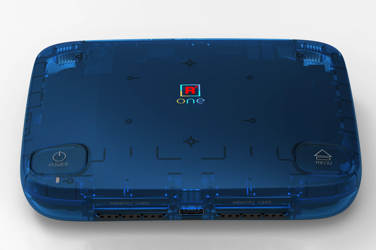
Gaming hardware manufacturer Retro Remake has recently launched the SuperStation ONE FPGA-based gaming console designed for retro gaming enthusiasts. The console is built around an Intel Cyclone V SoC FPGA and supports MiSTer FPGA core so users can replicate various retro platforms without modifications. The console has 128MB BGA SDRAM and uses a MicroSD Card and an M.2 SSD slot for storage. It features HDMI (up to 1536p/1440p), VGA, DIN10 for composite/RCA and component video output, along with 3.5mm analog and TOSLINK digital audio outputs. It also has built-in Wi-Fi, Bluetooth, Ethernet, and NFC integration supporting Zaparoo features. Other ports include dual PS1 SNAC ports for PlayStation controllers, three USB Type-A ports, an Ethernet port, and an IO expansion slot. The optional SuperDock adds a CD drive for PlayStation 1 discs, an M.2 SSD slot, and extra USB ports. SuperStation ONE specifications SoC FPGA – Intel/Altera Cyclone V SX (5CSXFC6D6F31I7N) […]
FOSDEM 2025 schedule – Embedded, Open Hardware, RISC-V, Edge AI, and more
FOSDEM 2025 will take place on February 1-2 with over 8000 developers meeting in Brussels to discuss open-source software & hardware projects. The free-to-attend (and participate) “Free and Open Source Software Developers’ European Meeting” grows every year, and in 2025 there will be 968 speakers, 930 events, and 74 tracks. Like every year since FOSDEM 2015 which had (only) 551 events, I’ll create a virtual schedule with sessions most relevant to the topics covered on CNX Software from the “Embedded, Mobile and Automotive” and “Open Hardware and CAD/CAM” devrooms, but also other devrooms including “RISC-V”, “FOSS Mobile Devices”, “Low-level AI Engineering and Hacking”, among others. FOSDEM 2025 Day 1 – Saturday 1 10:30 – 11:10 – RISC-V Hardware – Where are we? by Emil Renner Berthing I’ll talk about the current landscape of available RISC-V hardware powerful enough to run Linux and hopefully give a better overview of what to […]
Sonata v1.0 RISC-V platform combines AMD Artix-7 FPGA and Raspberry Pi RP2040 MCU, features CHERIoT technology for secure embedded systems
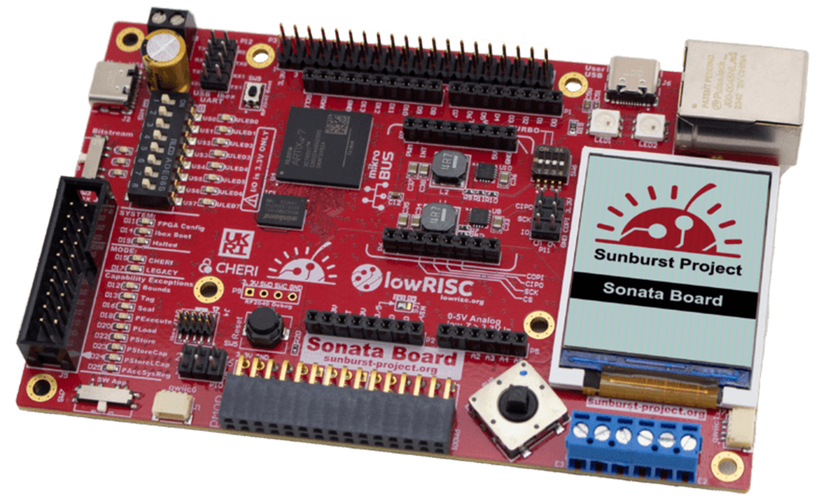
lowRISC has released Sonata v1.0, a stable platform developed under the Sunburst project. Designed for embedded systems engineers, Sonata supports CHERIoT technology, enabling features like compartmentalization and enhanced memory safety. It provides a reliable foundation for building secure embedded systems. CHERIoT is a security-focused technology built on lowRISC’s RISC-V Ibex core, based on CHERI research from the University of Cambridge and SRI International. It addresses memory safety issues like buffer overflows and use-after-free errors using CHERI’s capability-based architecture. The CHERIoT capability format includes permissions for memory access, object types for compartmentalization, and bounds to restrict accessible memory regions. These features enable scalable and efficient compartmentalization, making it suitable for securely running untrusted software in embedded systems. Sonata v1.0 leverages this architecture to isolate components like network stacks and kernels within the CHERIoT RTOS. The lowRISC Sonata v1.0 specifications: FPGA – AMD Xilinx Artix-7 (XC7A35T-1CSG324C) CPU – AMD MicroBlaze soft-core based on […]


