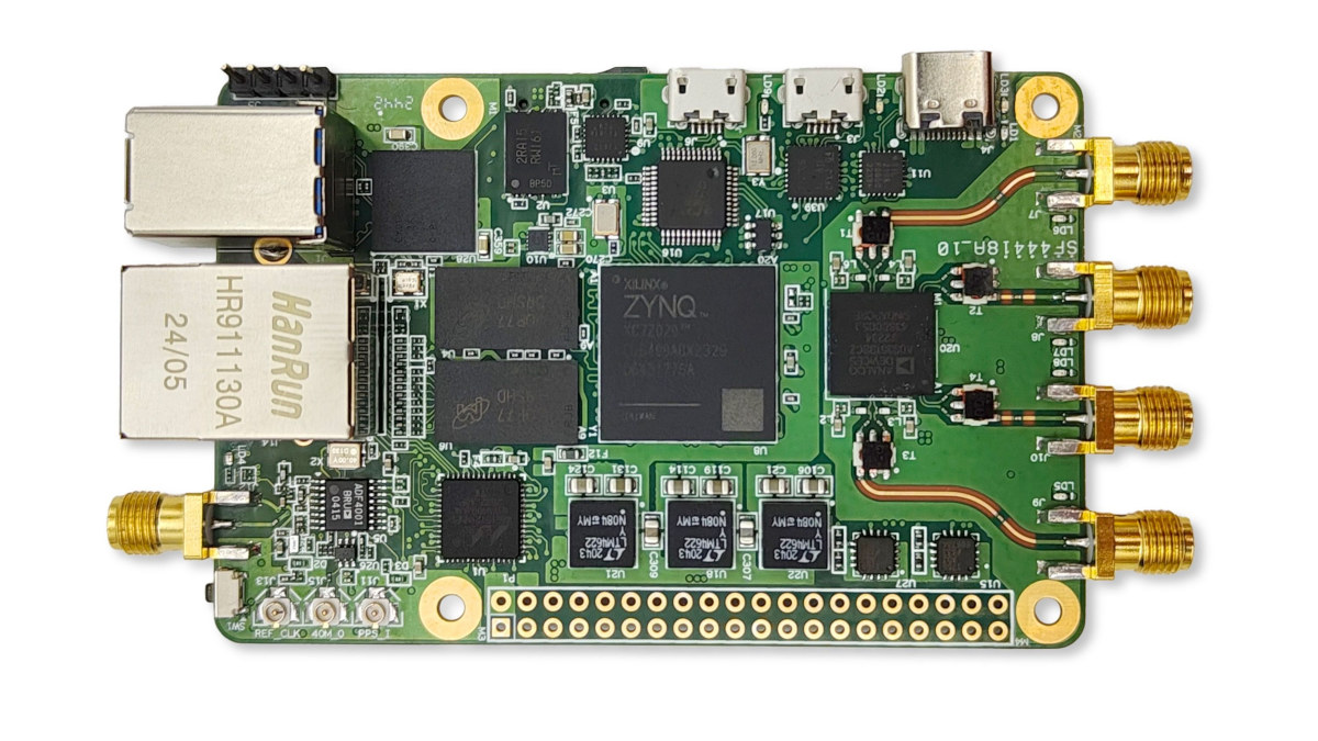
The SignalSDR Pro is a Raspberry Pi-sized SDR that brings a credit-card-sized twist to software-defined radios (SDRs). It is a compact, streamlined device suitable for tasks ranging “from signal processing and spectrum analysis to communication systems and beyond.” The SignalSDR Pro builds on the Analog Devices AD9361 radio transceiver and the AMD Zync 7020 SoC into a credit-card format reminiscent of Raspberry Pi single-board computers. The Raspberry Pi-sized SDR also features a 40-pin GPIO header for expansion with other hardware components and added functionality. The device offers a 70MHz – 6GHz tuning range, 12-bit sample rate, 61.44MHz RF bandwidth, and two full-duplex TX/RX channels via four I-PEX antenna connectors. It is also capable of emulating other SDR hardware such as the ADALM-PLUTO and USRP B210, making it easier to integrate into pre-existing workflows. The SignalSDR Pro is a mid-range alternative to entry-level SDR options such as the AntSDR E200, KrakenSDR, […]
AMD Versal RF Series adaptive SoCs target 6G wireless, aerospace, and electronics test equipment
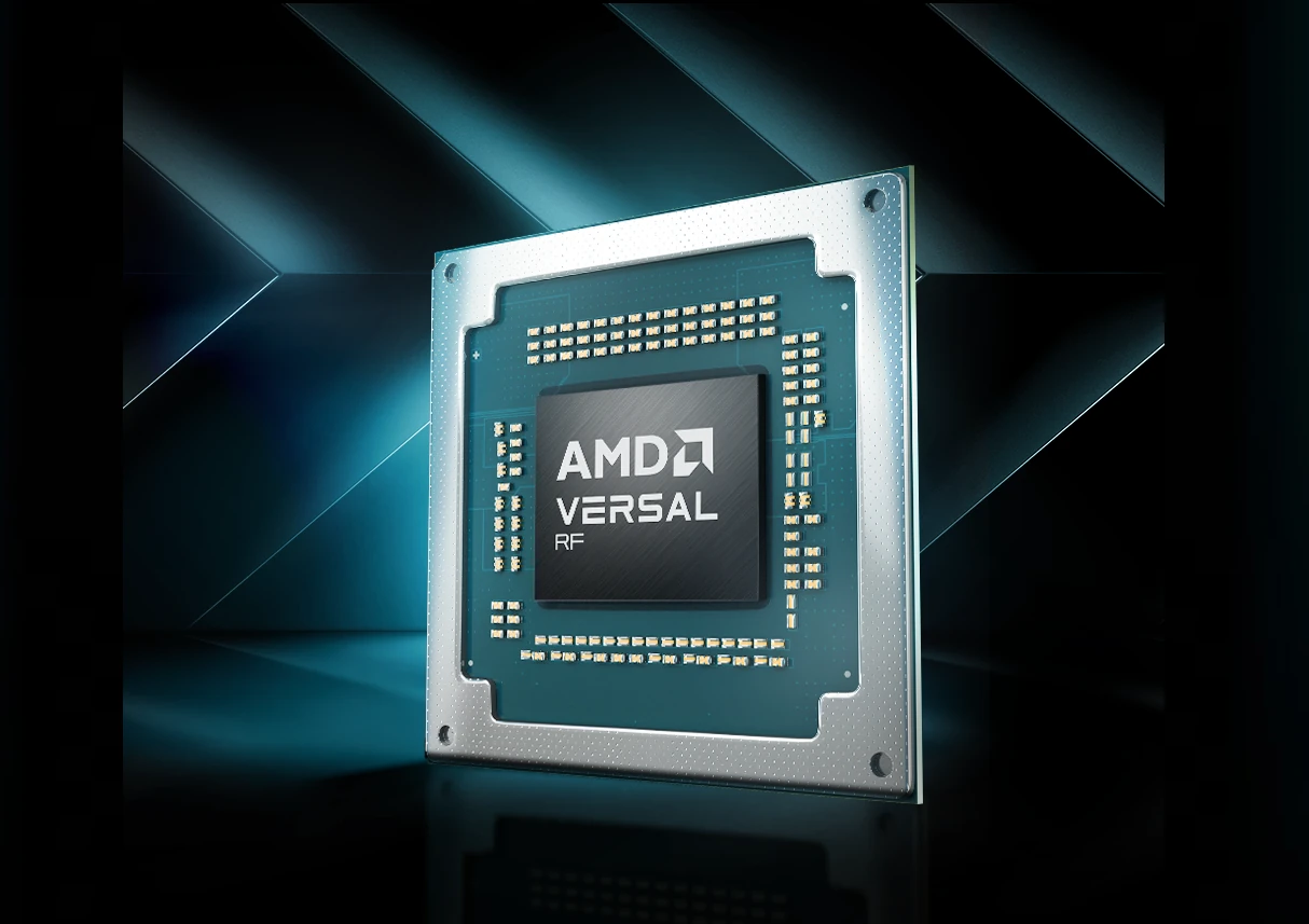
AMD Versal RF series adaptive system-on-chips (SoCs) combines Arm Cortex-A72 and Cortex-R5F hard cores with FPGA fabric and direct radio frequency (RF)-sampling data converters for pre-6G systems, wireless 6G testers, aerospace and defense applications like radars, and electronics test equipment such as multi-channel testers, oscilloscopes, and wideband spectrum analyzers. Built upon the Xilinx Zynq RFSoC devices, the AMD Versal RF Series supports wideband-spectrum with high-resolution thanks to up to sixteen 18 GHz, 14-bit RF ADCs with up to 32 GSPS and sixteen 14-bit RFV DACs up to 16 GSPS, and delivers 80 TOPS of DSP performance in a size, weight, and power (SWaP)-optimized design. The chips also integrate hard IP such as DDR5 memory controllers, 600 Gbps Ethernet, PCIe Gen5 x4, and various high-speed transceivers. AMD Versal RF Series adaptive SoCs key features and specifications: Processing System Application Processing Unit (APU) – Dual-core Arm Cortex-A72 with 48 KB/32 KB L1 […]
Lattice unveils Nexus 2 small FPGA platform, Lattice Avant 30 and Avant 50 mid-range devices, updated Lattice design software tools
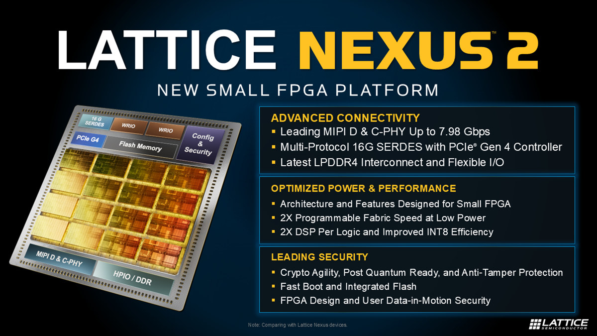
Lattice Semiconductors announced several new FPGAs and software tools at the Lattice Developers Conference 2024 which took place on December 10-11. First, the company unveiled the Nexus 2 small FPGA platform starting with the Certus-N2 general-purpose FPGAs offering significant efficiency and performance improvements in this category of devices. The Lattice Avant 30 and Avant 50 were also introduced as mid-range FPGA devices with new capacity options to enable edge-optimized and advanced connectivity applications. Finally, the company releases new versions of Lattice design software tools and application-specific solution stacks to help accelerate customer time-to-market such for edge AI, embedded vision, factory automation, and automotive designs with Lattice Drive. Let’s have a look at the highlights of each announcement. Lattice Nexus 2 small FPGA platform and Certus-N2 FPGA Highlights and benefits of the Lattice Nexus 2 small FPGA platform: Power Efficiency against similar class competitive devices Up to 3x lower power Up […]
$20 ATOMIC Display Base is a low-cost HDMI display driver for M5Stack’s ESP32-based Atom IoT controllers
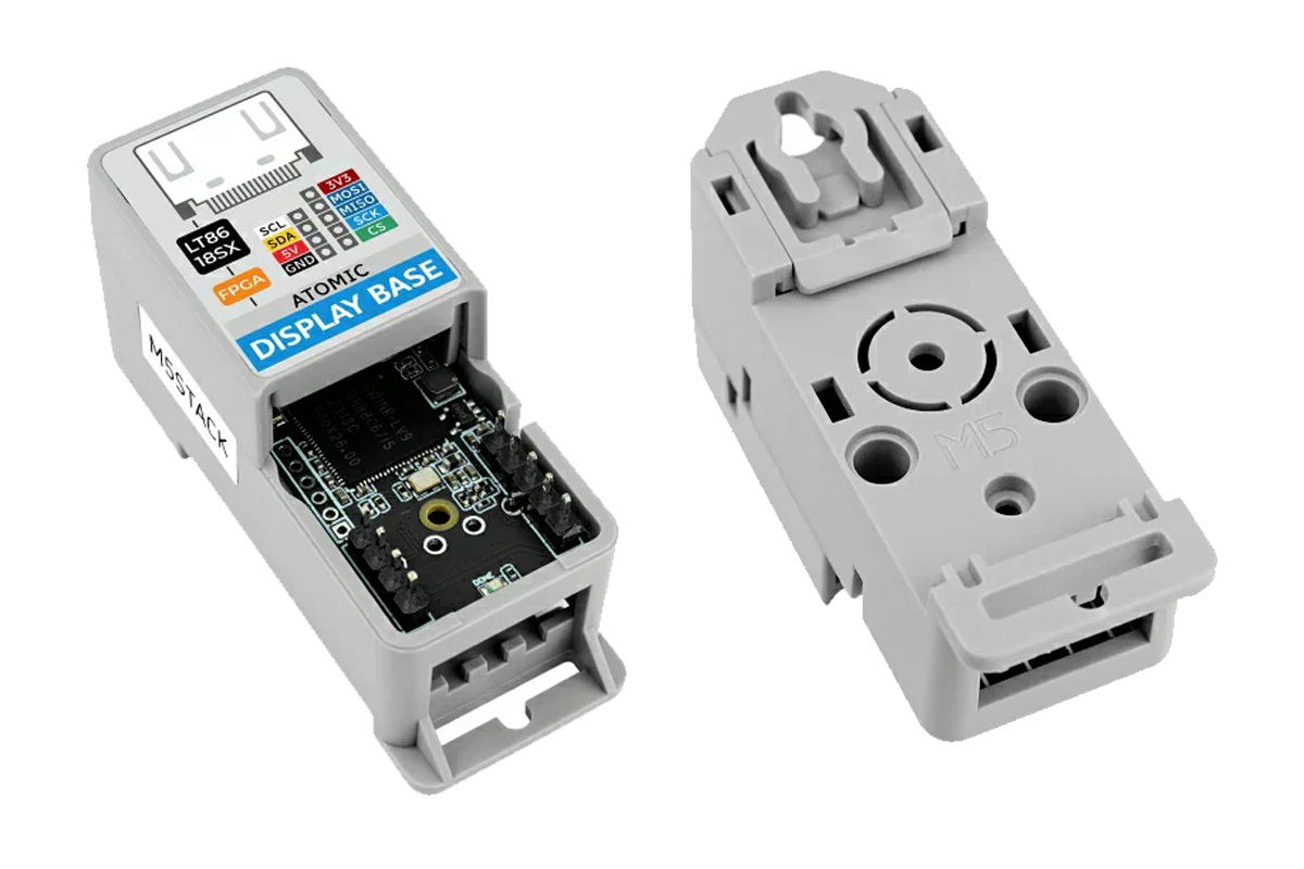
M5Stack has recently launched the M5Stack ATOMIC Display Base, an HDMI display driver designed to emulate traditional SPI TFT-LCD data output using Gowin GW1NR-9C FPGA and a built-in LT8618SX RGB-to-HDMI chip and designed to work with the company’s Atom IoT controller family based on ESP32 wireless microcontrollers. The module supports up to 720p (1280×720) image output with a 24-bit color depth and has an average frame rate of 12–16 FPS. Additionally, it can be paired with ATOM series hosts for various memory and application needs. These features make this compact device suitable for industrial control displays, smart home information screens, educational and conference presentations, and remote monitoring displays. The only downside of this device is that it requires a display with adaptive resolution scaling to avoid compatibility issues. M5Stack ATOMIC Display Base (HDMI display driver) specifications FPGA – Gowin GW1NR-9C (PDF datasheet) FPGA with 8,640 LUTs used to simulate SPI TFT-LCD data […]
Black Friday and Cyber Monday 2024 – International deals and coupons
While Black Friday and Cyber Monday used to be a US-only event, it changed many years ago, and we’ve been writing about international Black Friday and Cyber Monday deals and coupon codes since 2014, since a large portion of our audience cannot benefit from promotions on Amazon’s Black Friday and Cyber Monday events that will take place from November 21 until December 2 this year. So I’ve gathered some international Black Friday and Cyber Monday 2024 deals and discount coupon codes from relevant manufacturers and popular online stores such as Aliexpress, Banggood, and others. Aliexpress Black Friday and Cyber Monday event Aliexpress’ Black Friday and Cyber Monday 2024 event has already started. There are three periods: Nov 19-21 PST – Warm Up event where users can find and add items to the cart before purchasing during the main event. Nov 22-30 PST – “On Sale” event with discounts up to […]
High-speed data acquisition with Raspberry Pi Pico 2’s HSTX interface and HDMI to USB 3.0 video capture dongle
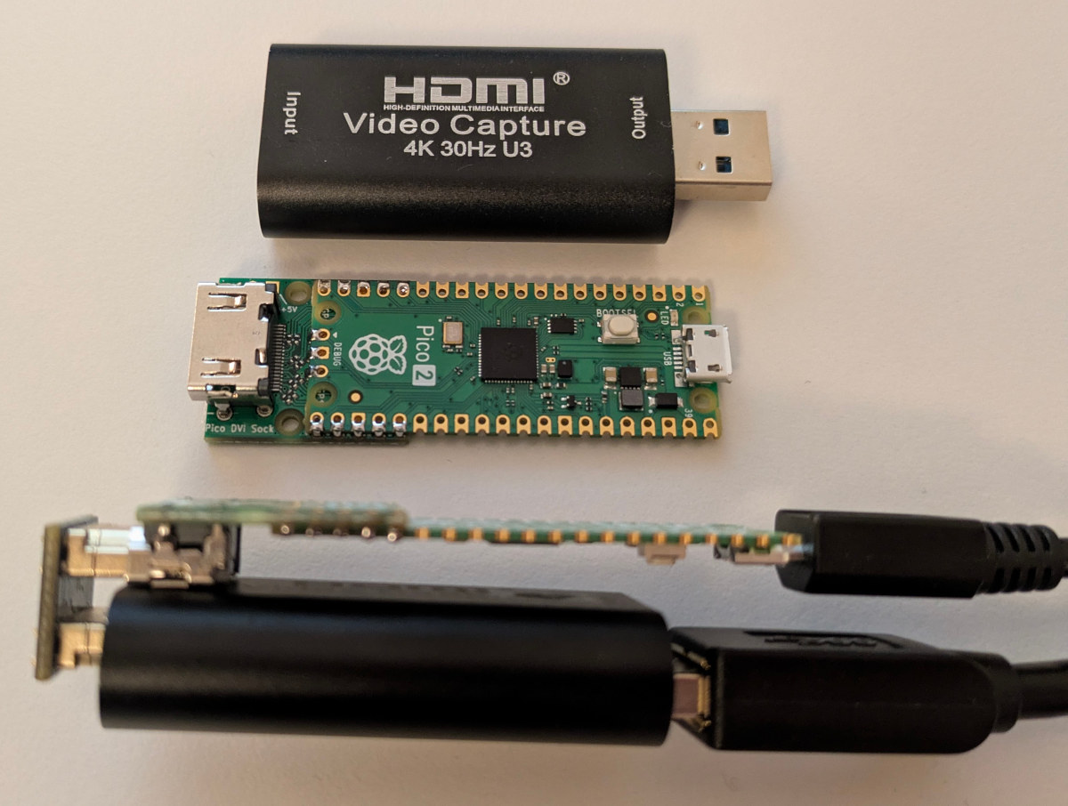
We previously explained the HSTX high-speed serial transmit interface of the Raspberry Pi RP2350 microcontroller was mostly useful for video outputs and display interfaces since it can only transmit, and not receive data. But Steve Markgraf found another use case for the HSTX interface – high-speed data acquisition – combining a Raspberry Pi Pico 2 board with the DVI Sock board for Pico and one of those cheap MS2130-based HDMI to USB 3.0 video capture dongles. He managed to stream out up to 75 MB/s of real-time data from an overclocked RP2350 to a host computer with a USB 3.0 port. The Adafruit Feather RP2350 HSTX board should also work, but also not been tested. Steve’s “hsdaoh-rp2350” data acquisition over HDMI firmware is based on the dvi_out_hstx_encoder example from Raspberry Pi using the HSTX interface for DVI output and code by Shuichi Takano implementing the HDMI data island encoding required […]
AMD Versal Premium Gen2 SoC FPGA family features Arm Cortex-A72/R5F cores, high-end FPGA fabric, PCIe Gen6, CXL 3.1 interfaces
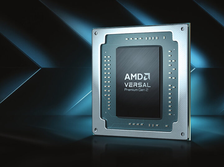
AMD Versal Premium Series Gen 2 SoC FPGA combines dual-core Cortex-A72 and dual-core Cortex-R5F processors with high-end FPGA fabric with up to 3.2 million logic cells and CXL 3.1 (Compute Express Link), PCIe Gen6, and DDR5/LPDDR5X high-bandwidth interfaces for data center, communication equipment, test & measurement, and aerospace & defense data-intensive applications. AMD Versal Premium Gen2 specifications: CPU cores Dual-core Arm Cortex-A72 application core, 48 KB/32 KB L1 Cache w/ parity & ECC; 1 MB L2 Cache w/ ECC Dual-core Arm Cortex R5F, 32 KB/32 KB L1 Cache, and 256 KB TCM w/ECC Memory – 256MB on-chip with ECC FPGA fabric System Logic Cells – Up to 3,273,480 LUTs – Up to 1,496,448 DSP Engines – Up to 7,616 Interfaces connected to CPU cores 2x Ethernet 2x UART, 2x SPI, 2x I2C 2x CAN-FD 1x USB 2.0 FPGA memory, interfaces, I/Os, and transceivers Up to 327 Mbit memory @ 273 […]
Signaloid C0-microSD is an iCE40UP5K FPGA SoM in the microSD card form factor (Crowdfunding)
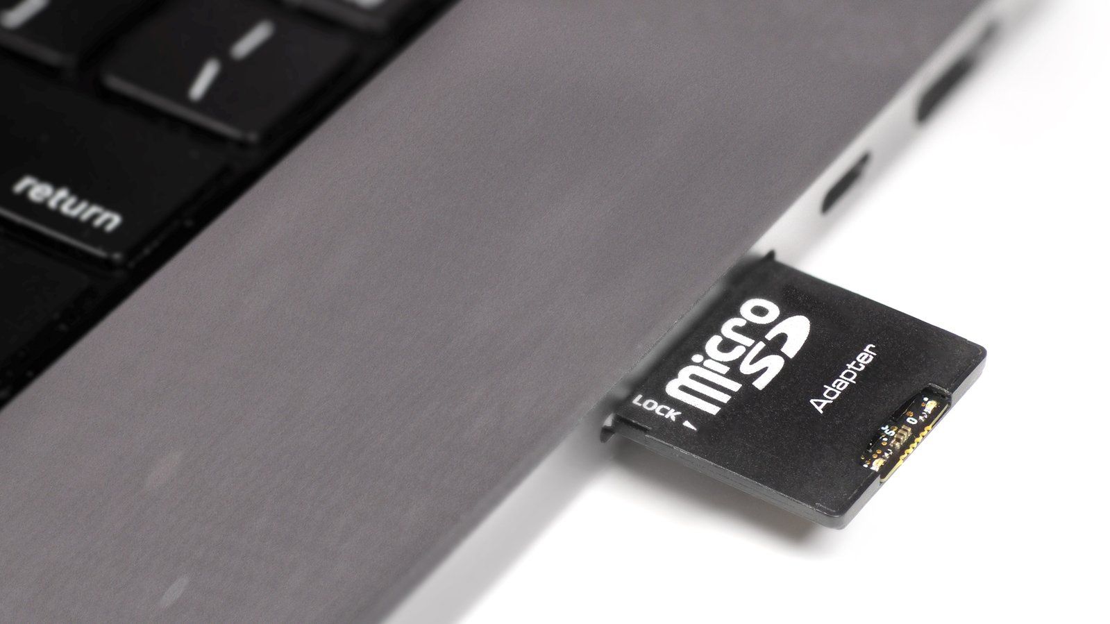
Cambridge-based hardware and cloud computing company, Signaloid has begun crowdfunding for the C0-microSD – a tiny, programmable iCE40UP5K FPGA system-on-module (SoM) in a microSD card form factor. It comes preloaded with a RISC-V softcore and users can also load custom FPGA designs onto the board. Part of the Signaloid C0-microSD’s unique appeal is its SD card form factor, which allows it to fit in unused full SD or microSD slots. This allows the implementation of FPGA-based hardware acceleration in systems without traditional expansion interfaces like PCIe M.2 slots. It can also be interfaced with as a standard SD block device and used to bring hardware-accelerated data processing to existing industrial automation, manufacturing, and robotics systems. The iCE40UP5K FPGA SoM has two main use cases: a hot-pluggable FPGA module or a hot-pluggable RISC-V co-processor module. The SD interface allows you to load custom FPGA bitstreams and applications onto the module from […]


