
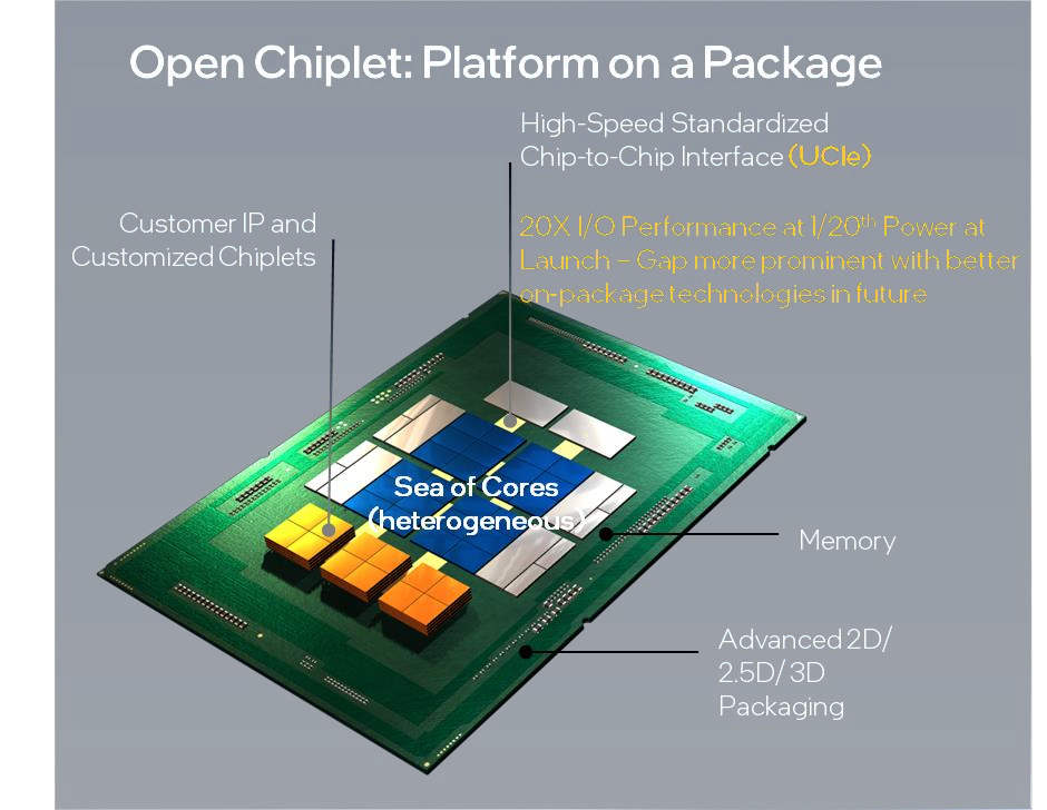
We first heard about Chiplet, chips that gather IP or chips from different vendors into a single chip, in 2020 with the now-defunct zGlue’s Open Chiplet Initiative, but the term recently came back to the forefront last month with Intel’s investment into the “Open Chiplet Platform” that aims to offer a modular approach to chip design through chiplets with each block/chiplet customized for a particular function.
It turns out there’s now an official standard called the Universal Chiplet Interconnect Express (UCIe) whose specification defines the interconnect between chiplets within a package, and not only backed by Intel, but also AMD, Arm, ASE, Google Cloud, Meta, Microsoft, Qualcomm, Samsung, and TSMC.
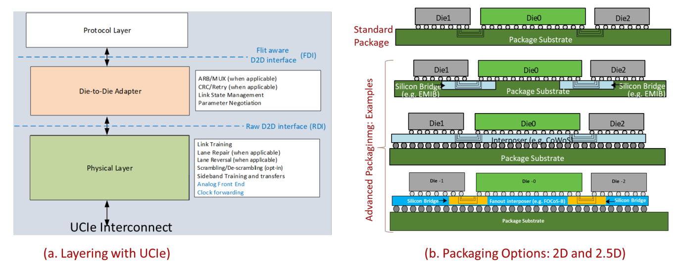
UCIe defines the Physical Layer (Die-to-Die I/O) and protocols to be used for the chiplet interfaces, currently PCIe and CXL (Compute Express Link), but more protocols will be added to the specification in the future.
The goal is to provide the ability to mix-and-match package dies from different fabs, different designs/architectures, and different packaging technologies. The Universal Chiplet Interconnect Express says the initiative is to address the projected growing demands of compute, memory, and storage in the cloud, edge, enterprise, 5G, automotive, high-performance computing, and hand-held segments.
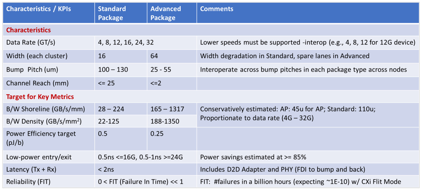
The white paper about UCIe also mentions high-bandwidth, low-latency, power-efficient, and cost-effective on-package connectivity with more detailed metrics available from the table below.
There’s already been SoCs with IP from different vendors for years, for example, Arm cores are often combined with Imagination or Vivante GPU, but the new standard should just make it easier, and we may see more and more chips mixing x86, RISC-V, and/or Arm plus other IPs.
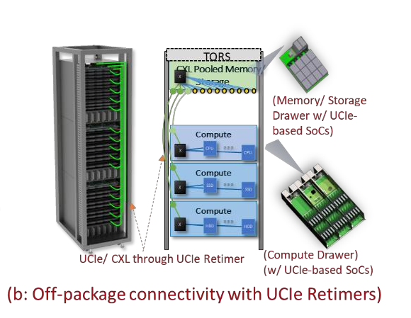
Anandtech notes that UCIe offers a solution that’s a bit like PCIe expansion cards in a computer but at the silicon level. The UCIe specification also allows retimers to transfer UCIe over much longer distances, so it could be used off-package in computer-on-module or memory/storage modules inserted into server racks at the cost of lower latency and power benefits due to the extra distance.
More details can be found on the official website.

Jean-Luc started CNX Software in 2010 as a part-time endeavor, before quitting his job as a software engineering manager, and starting to write daily news, and reviews full time later in 2011.
Support CNX Software! Donate via cryptocurrencies, become a Patron on Patreon, or purchase goods on Amazon or Aliexpress


I think that in this way chipmakers will divide better they work and skills, for example there could be one chiplets maker for DDR RAM and other chipmakers will use all that module