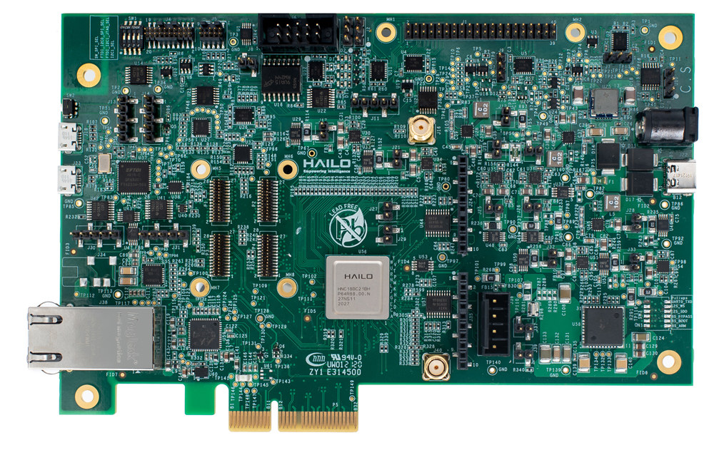
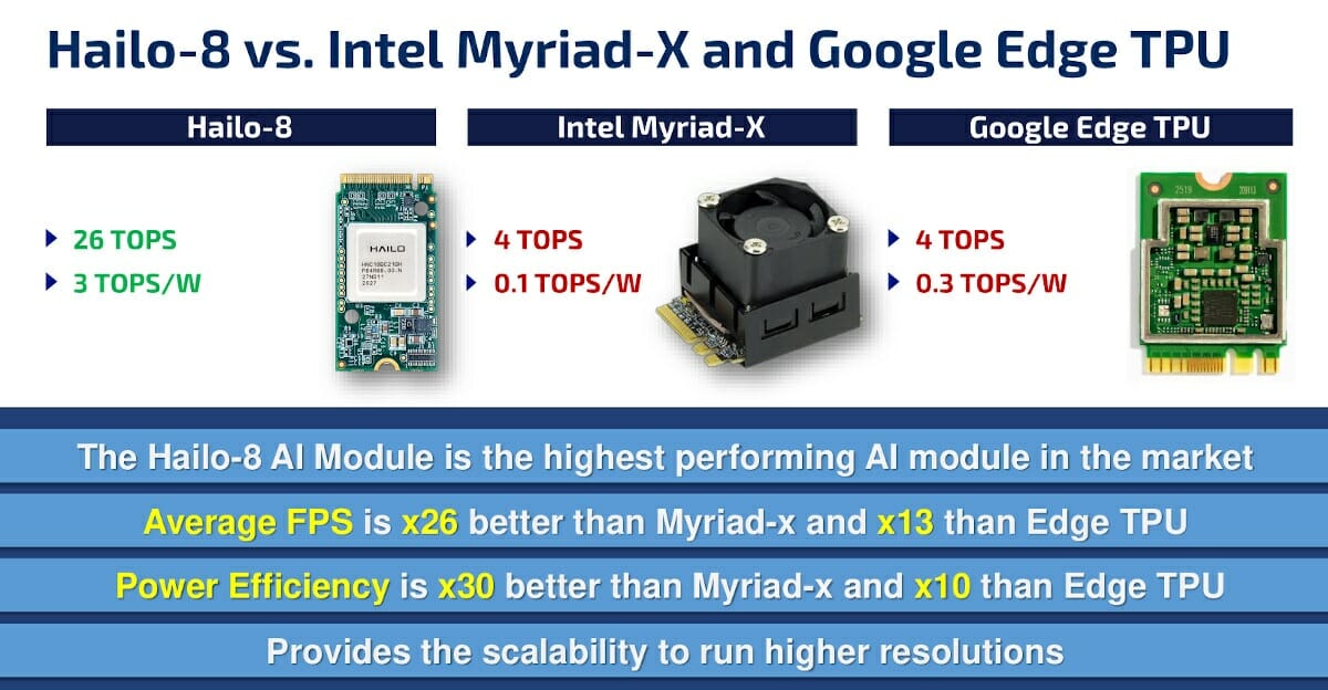
Last week we wrote about Hailo-8 M.2 card delivering up to 26 TOPS of AI performance, and comparing well against Google Edge TPU and Intel Movidius Myriad X both in terms of footprint, performance, and efficiency.
I’ve since then had a conference call with Liran Bar, VP of Business Development for Hailo, where we had time to discuss more about Hailo’s AI solutions, and how to interpret & understand AI benchmarks that may be misleading in many instances.
Hailo-8 Architecture
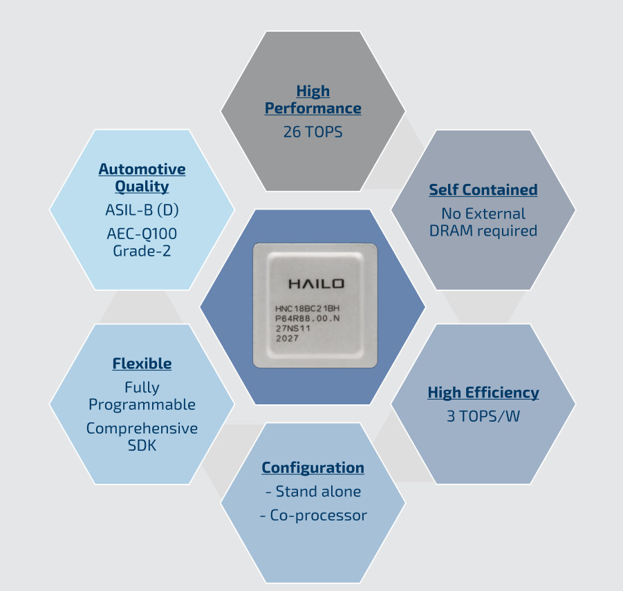
In the first post, we noted the chip managed to get the extra performance and efficiency thanks to a “proprietary novel structure-driven Data Flow architecture instead of the usual Von Neumann architecture”. But that’s a bit abstract, so Liran told me one of the key reasons for the performance improvement is that RAM is self-contained without the need for external DRAM like other solutions. This decreases latency a lot and reduces power consumption.
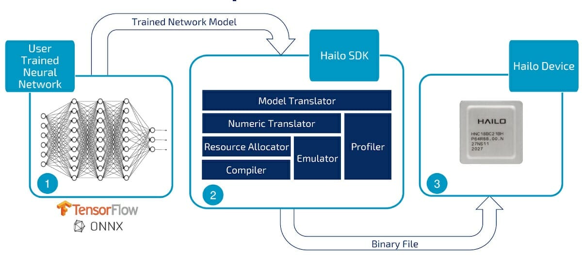
Internally, the Hailo-8 chip is comprised of three types of blocks with control, memory, and compute which are assigned to various layers of the neural network graph as shown in the animation below.
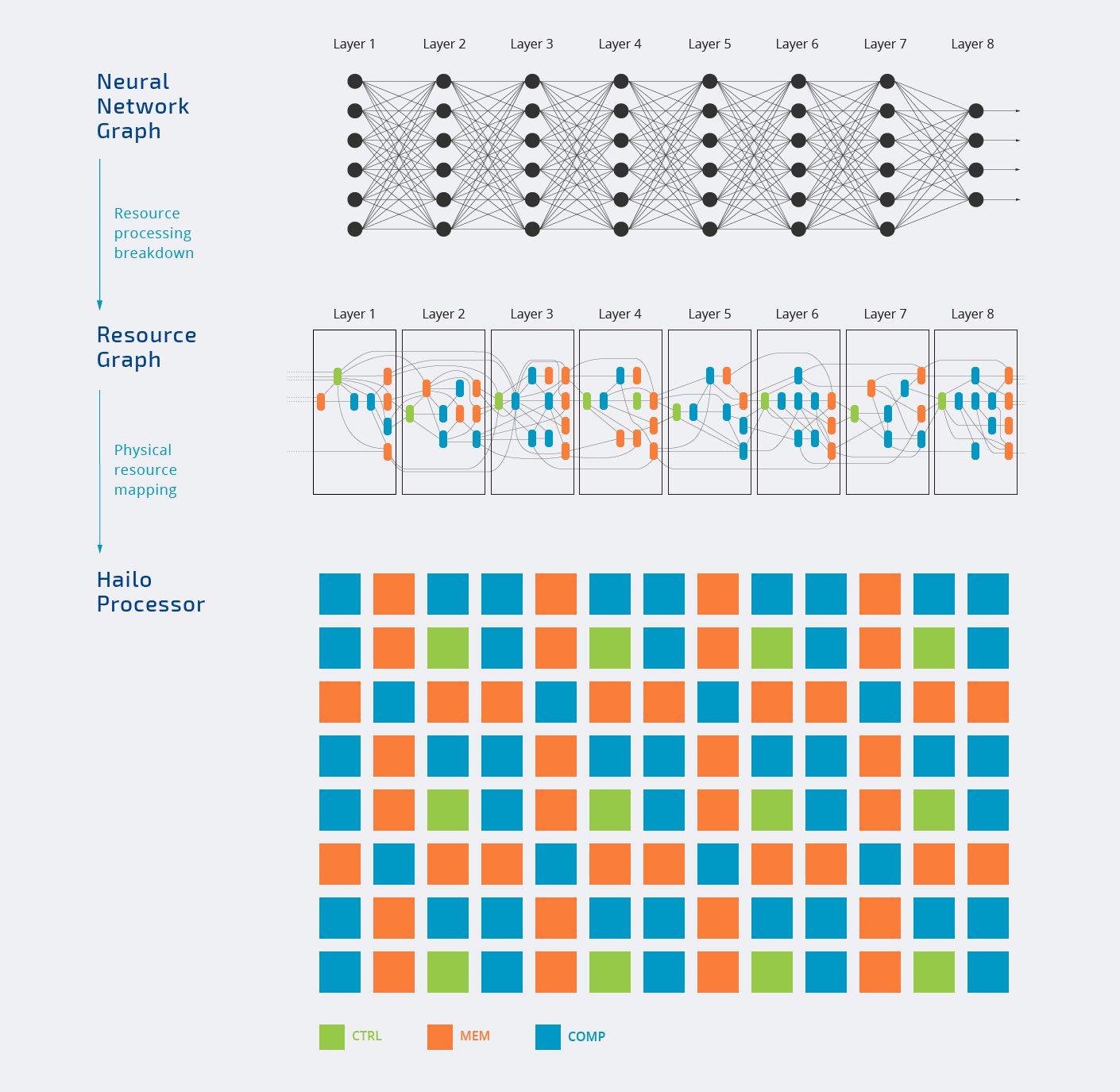
All processing takes place internally happens in the chip. You’ll also notice not all blocks are assigned, and that’s normal since every AI workload will only use parts of the AI accelerator. That’s also why the frequently TOPS number touted by companies is mostly a “marketing plot”.
The top diagram also shows Hailo-8 can be used in both standalone mode or a co-processor. Most companies will interface the chip with a more powerful host processor to handle other tasks, but in theory, it’s also possible to use Hailo-8 by itself.
Hailo-8 Development Tools
The company provides an Hailo-8 evaluation board with PCIe edge connector, Gigabit Ethernet, audio, USB ports, I2C & UART interfaces, GPIO as well as two MIPI CSI camera interfaces. It’s meant to be plugged into a computer where you can use the development tools for TensorFlow or ONNX training, before getting the model through Hailo SDK to convert data and allocate resources as shown in Hailo-8 animation we presented above.
If you’ll like to get the hardware and software development tools, you’ll need to provide company and project details. I asked whether Hailo would make those more broadly available, and Liran answer eventually, but right now they are focusing on commercial projects. Hailo is an Israeli startup founded in 2017, and while they received a 88 million investment from NEC, ABB, and other investors, the company is likely not making any profit right now. Hailo also got requests from universities, but they had to decline since as a small company they don’t know the resources to provide support. If you have a project you can enquire on the product page.
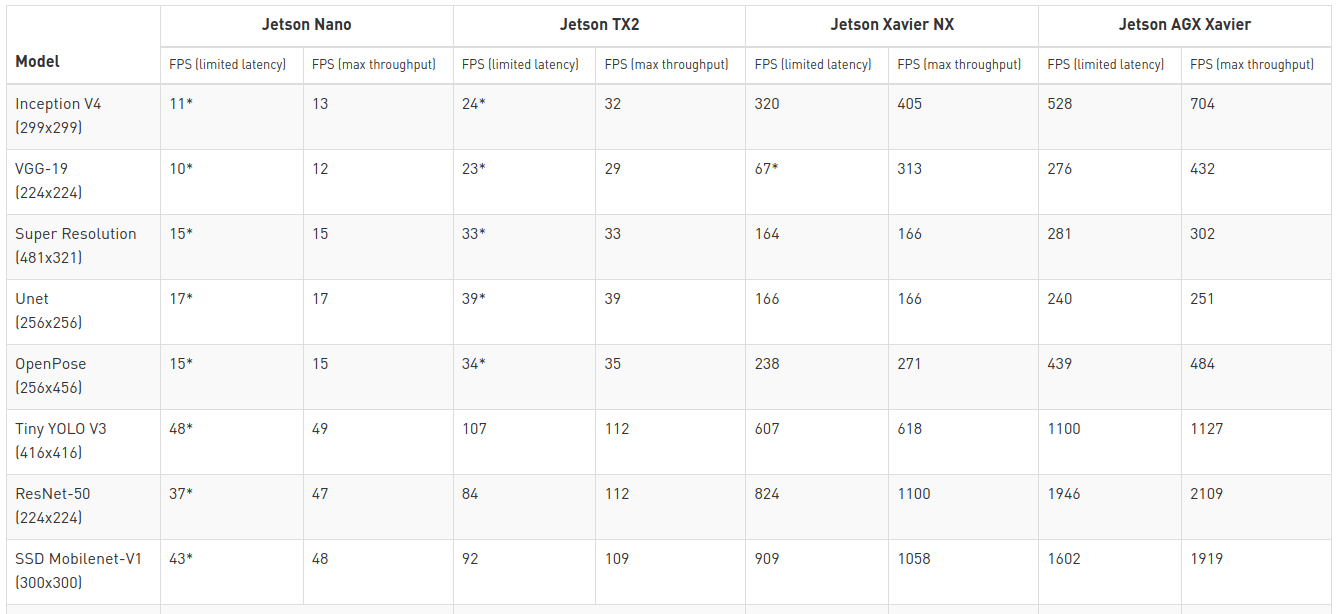
Hailo-8 vs NVIDIA Jetson
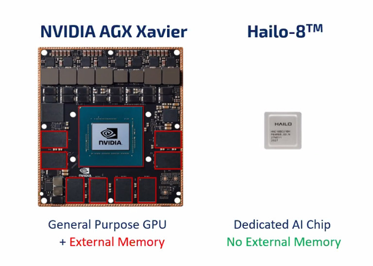
In their press release, the company focused on comparison with Edge TPU and Myriad X chips, but based on TOPS number, Hailo-8 performance is much closer to a solution like NVIDIA AGX Xavier. As you can see from the photo above the form factor is way smaller, and could be critical to your application if you used multiple AI accelerators in one application. That’s not to say both are the same as NVIDIA AGX Xavier is more flexible since you can also do training on the platform, while Hailo-8 is only made for low-power inference which it does at 20 times the power efficiency.
You may wonder why there’s a note about the batch size. That’s because Jetson Xavier NX relies on both an NVIDIA Volta GPU, and NVDLA engines, and GPUs perform better with highly parallel tasks, so the batch sized is configurable and impacts both performance and efficiency.
Understanding AI Benchmarks
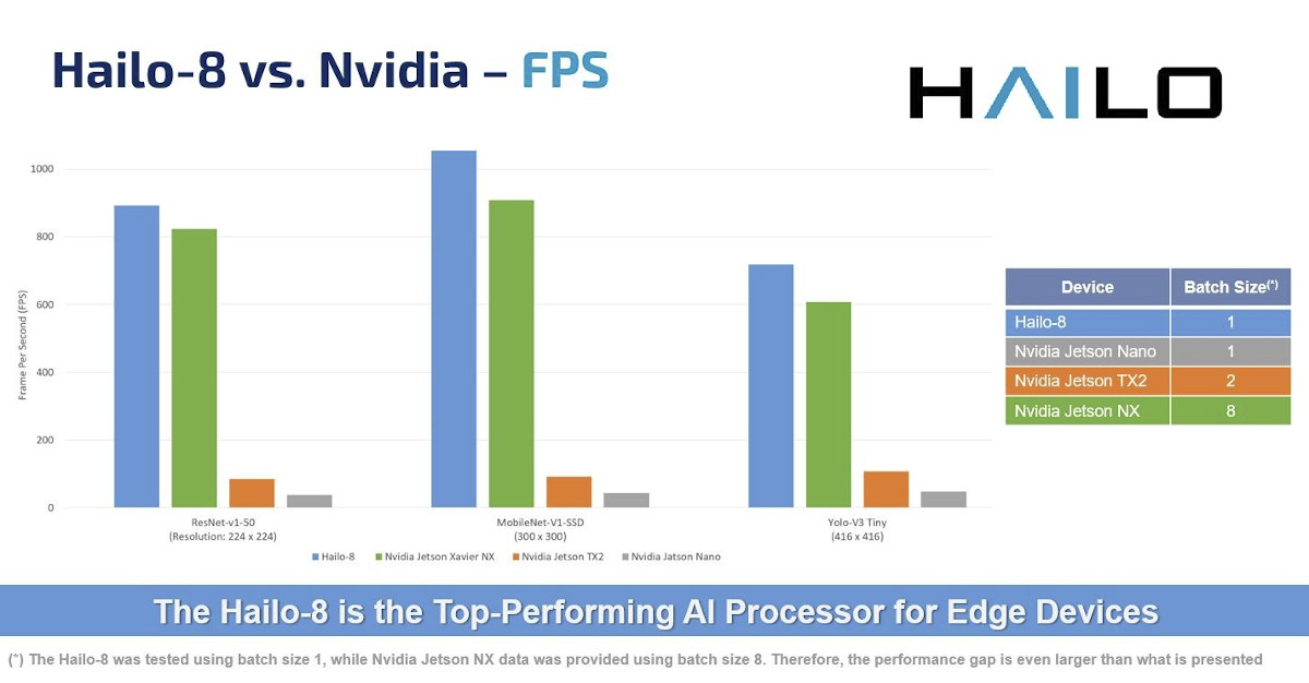
AI chips companies like to float TOPS numbers to show the maximum theoretical performance of their chips. But in practice, those are just for marketing. For example, Hailo-8 is advertised with 26 TOPS, while Google Edge TPU is said to handle up to 4 TOPS. That’s six times the performance, but when running actual benchmarks, Hailo is 13 times faster than Edge TPU on average due to architectural differences. As we noted above, no AI workload will use all resources from the chip up to the advertised TOPS.
So TOPS numbers should always be taken with a grain of salt, and you may want to rely on benchmarks instead, but there are pitfalls here as well. If we look at Jetson Xavier AGX benchmarks, we can see the batch size is clearly shown.
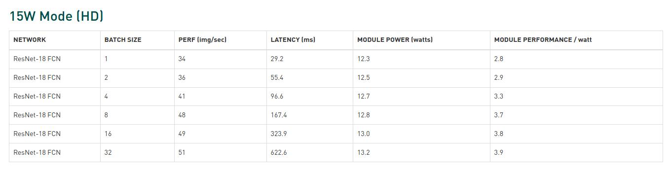
So that makes comparison a bit more difficult. NVIDIA still states “the minimum latency throughput results were obtained with the maximum batch size that would not exceed 15ms latency (50ms for BERT) — otherwise, a batch size of one was used.”. That true except for results marked with * where the latency is over 15ms.
Standard benchmarks can still help, but one must be attentive to details. MobileNet-v1 SSD is typically run with an image size of 300×300, but Google decided to run the benchmark with smaller 224×224 images on the Edge TPU.
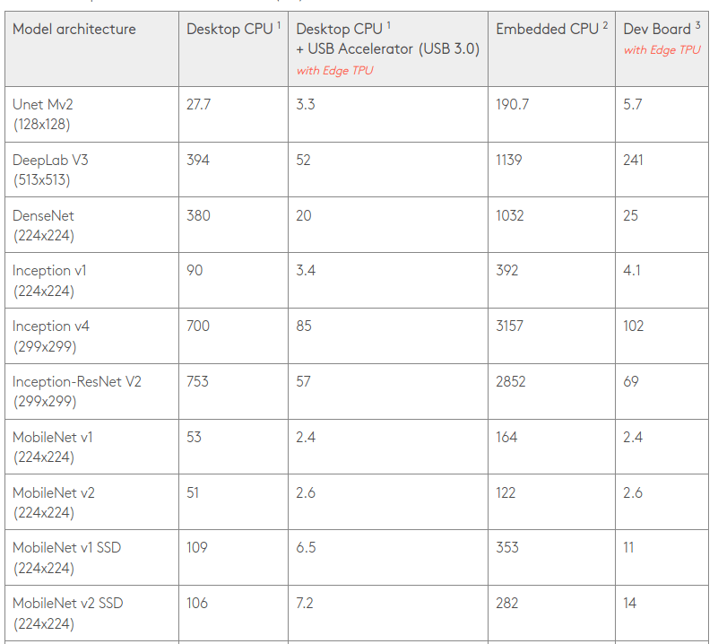
The company also shows results for a Desktop CPU with and without USB accelerator, and the same for an embedded CPU. The latter is a quad-core Cortex-A53 processor, but the “Desktop CPU” is a ~$4,000 Intel Xeon Gold 6154 18-core/36-thread processor with 200W TDP. So when you see benchmarks showing TOPS per watt for the accelerator, it becomes much less relevant when connected to a 200W processor…
Google writes “An individual Edge TPU is capable of performing 4 trillion operations (tera-operations) per second (TOPS), using 0.5 watts for each TOPS (2 TOPS per watt)”. But based on the benchmark tricks explained above, and other calculation, Hailo disputes Google claims of 2 TOPS/W, and instead claims an efficiency of only 0.3 TOPS/W, making Hailo-8 ten times more power efficient!
[Update: here’s how the TOPS/W calculation was done:
- Determine a workload (for instance Mobilenet V2) ==> this defines the number of operations per frame of a given size (e.g. 224×224) (A)
- use the actual measured throughput in frames-per-second (B)
- use the actual measured power consumption (C)
- multiply the number from A by the number from B and divide by the number from C (with proper units) ==> this gives TOPS/W
- Example – MobileNet V2 – according to edge TPU M.2 datasheet:
- MobileNet V2 TOPS / frame: 300 M MAC per frame = 600 M OPS per frame = 0.6 GOP per frame = 0.0006 TOP per frame (A) (reference, see figure 5)
- Throughput: 416 fps (B) (reference: coral.ai M.2 datasheet, table 3)
- Power: 1.4W (C) (reference: coral.ai M.2 datasheet, table 3)
- It follows that: 0.0003 * 416 / 1.4 = 0.178 TOPS/W in this case
- Please that all of the above relies on edge-TPU published information]
The best is not to believe anyone, and if possible, get an evaluation board for each target platform and run your own AI workloads.

Jean-Luc started CNX Software in 2010 as a part-time endeavor, before quitting his job as a software engineering manager, and starting to write daily news, and reviews full time later in 2011.
Support CNX Software! Donate via cryptocurrencies, become a Patron on Patreon, or purchase goods on Amazon or Aliexpress