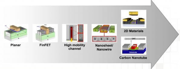
TSMC provides an update to its process technology roadmap at the Online Technology Symposium and OIP Ecosystem Forum with the 5-nanometer (N5) technology having entered mass production earlier this year, and an enhanced N5P version coming in 2021 offering further speed gain and power improvements, followed by N4 process (also 5nm) starting “risk production” in Q1 2021.
But the most interesting part was looking ahead to 3nm and 2nm process technologies. TSMC’s N3 (3nm) process aims to provide a 15% performance gain, up to 30% power reduction, and logic density gains up to 70% over N5.
N3 will rely on 13.5nm extreme UV (EUV) technology and be first used by UK based AI chip designer Graphcore. Their current AI chip – Colossus Mk2 Intelligence Processing Unit (IPU) – is built on 7nm with 59.4 billion transistors, and the next 3nm chip should have over 100 billion transistors. Anandtech managed to get a quote from Nigel Toon, CEO & co-founder at Graphcore, about the announcement:
Graphcore was first to build a completely new kind of fully programmable processor, designed from the ground up for machine intelligence. Many of the innovative features of our IPU architecture and the high yields we see even at the cutting edge of the latest process node, are testament to the close technology partnership we enjoy with TSMC. With 59.4Bn transistors, and built using the latest TSMC 7nm technology, the MK2 IPU, which we announced in July, is the world’s most sophisticated processor. Each GC200 IPU has 1472 independent processor cores and an unprecedented 900MB of In-Processor memory delivering an 8x step up in real world performance vs. our MK1 products. We continue to work closely with TSMC as one of their technology innovation partners to explore the advantages of new process nodes and techniques, including N3, so we can continue to deliver more performance improvements to enable our customers to make new breakthroughs in AI.”
Those are clearly chips to be used in the cloud, and not “at the edge”. I suppose TSMC 3nm process will come to high-end consumer-grade processors a little later in 2023.

Those new technologies require a lot of investment and manpower, with TSMC building a new R&D center to be completed in 2021 and housing 8000 scientists and engineers. This explains why so many silicon vendors had to go fabless as years passed.

Jean-Luc started CNX Software in 2010 as a part-time endeavor, before quitting his job as a software engineering manager, and starting to write daily news, and reviews full time later in 2011.
Support CNX Software! Donate via cryptocurrencies, become a Patron on Patreon, or purchase goods on Amazon or Aliexpress


