With open ISAs like RISC-V, it’s become easier – provided you have the skills – to develop or customize your own SoC using RTL files, compile it with EDA tools, and run the resulting bitstream on an FPGA. But if you ever wanted to get an actual chip that would become more complex, as you’d need to request a process design kit (PDK) from a foundry, and pay for the manufacturing cost, which amounts to at least several thousand dollars for older process nodes.
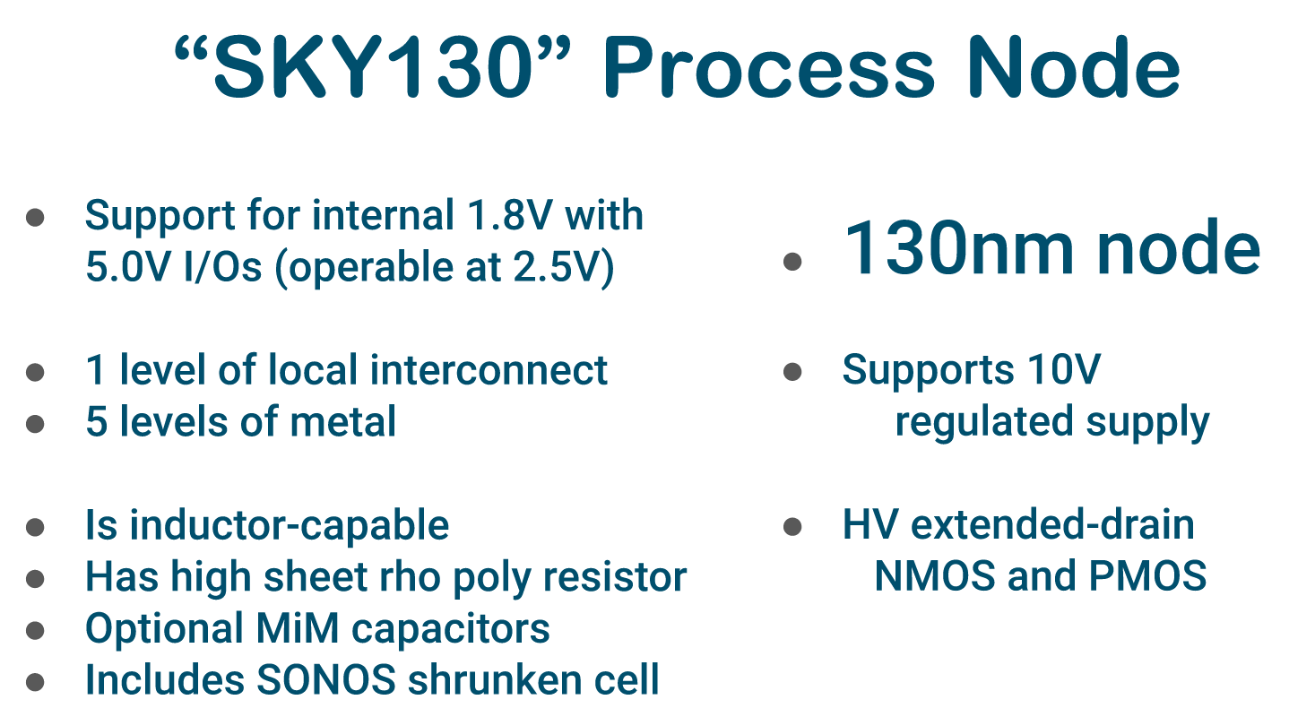
But the FOSSi (Free and Open Source Silicon) Foundation has good news with Tim Ansell of Google announcing the SkyWater PDK, the first manufacturable, open-source process design kit. There are other open-source PDKs, but they aren’t manufacturable and/or only support older 0.35/0.5 micron nodes. The SkyWater PDK allows you to produce chips with the SkyWater foundry in the 130nm node.
That’s a big improvement since you have access to an open-source PDK that’s manufacturable. but you’d still need money to pay for production. Or do you? Actually, you don’t as Google and eFabless are providing completely free of cost chip manufacturing runs for up to 100 ICs per design starting in November this year and multiple more in 2021. You just need to come up with an open-source chip design, and there aren’t other requirements although there’s a limit of 40 projects.
You’ll find more details in the video below (slides: here).
To get started, access the SkyWater PDK repository on Github that provides:
- Documentation around the design rules required to create manufacturable devices on the SKY130 Process Node.
- EDA tooling support files for multiple open source and proprietary design flows.
- Primitive cell libraries and models for creating analog designs.
- Multiple standard digital cell libraries covering a range of different use cases.
- Multiple documented examples of using the PDK including a RISC-V SoC design
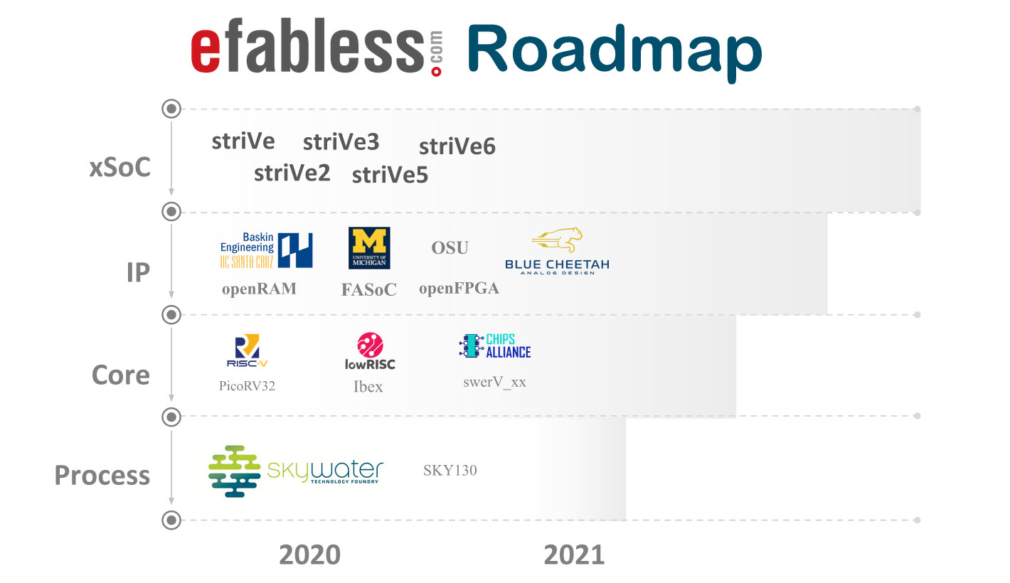
A roadmap from the presentation slides shows there are already various designs scheduled for production using SkyWater SKY130 130 nm process.

This includes striVe family of full ASIC reference designs with open-source RAM, FPGA, PicoRV32 & lowRISC ibex RISC-V cores, and more.
Via Hacker News

Jean-Luc started CNX Software in 2010 as a part-time endeavor, before quitting his job as a software engineering manager, and starting to write daily news, and reviews full time later in 2011.
Support CNX Software! Donate via cryptocurrencies, become a Patron on Patreon, or purchase goods on Amazon or Aliexpress


This is really cool, but a 130nm node is almost 20 years old. What is possible to do with a node like that in this days?
I think some MCUs are still manufactured in 130nm or slightly lower process node.
I did a search and Sifive low power MCU is 180nm, 130nm. So just as Jean Luc says above.
Examples for other 130 nm and 90 nm designs
(a) 32 bit Integer ALU, about 5 GHz :
https://www.researchgate.net/publication/2978897_5-GHz_32-bit_integer_execution_core_in_130-nm_dual-Vsub_T_CMOS
(b) To my knowledge the single-precession SPE-FPU in ibms well known Cell-processor was a 95 nm node design ;
https://ieeexplore.ieee.org/document/1610620
(c) If you like you could make a new FPGA :
https://www.researchgate.net/publication/321745323_FPGA_with_Improved_Routability_and_Robustness_in_130nm_CMOS_with_Open-Source_CAD_Targetability