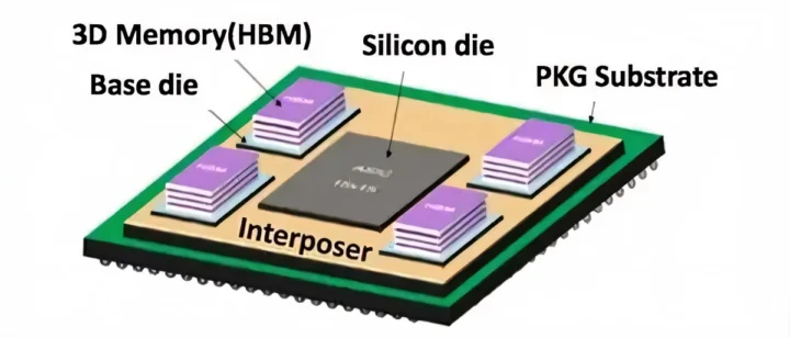
Connections between chips have become increasingly complex, and applications with higher frequency and speed requirements may not make use of traditional PCB technology. That’s where the interposer PCB, a new type of PCB comes into play. PCBWay has the capability to manufacture high-layer, high-order PCBs, and even successfully developed a 24-layer, 6-order arbitrary interconnection HDI PCB.
The interposer PCB is a highly precise, high-density interconnect (HDI) PCB that allows for a higher wiring density per unit area compared to traditional PCBs. HDI PCBs are characterized by features such as micro vias, finer lines and spaces, higher connection pad density, and the use of blind and buried vias. These features enable the miniaturization of electronic devices by allowing more functionality to be packed into a smaller space.
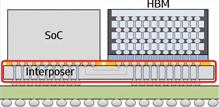
The design characteristics of this PCB include inner layers connected to the outer layers through laser microvias and dense routing, resulting in a multi-structure with BGA connections on the top side and pad connections on the bottom side as shown in the illustration below.
Some advantages of using an interposer PCB include:
- Higher connection speeds and reliability for semiconductor products.
- Improved signal integrity and lower power consumption since signal pins can be directly connected to the interposer layer, reducing the length of signal transmission paths
- The interposer layer also serves a thermal management role reducing the chip’s temperature.
- Enables connection between heterogeneous integrated circuits by placing them on the same interposer layer, thereby enhancing the overall performance and efficiency of semiconductor products.
As a result, interposer PCBs are widely used in fields such as high-performance computing, artificial intelligence, data centers, and communications.
PCBWay recently demonstrated their ability by manufacturing a high-precision circuit product using the 24-layer, 6-order Anylayer HDI PCB and showcasing their high-layer, high-order interposer PCB manufacturing service.
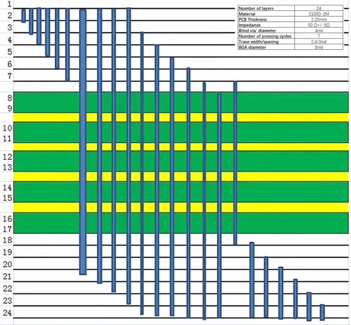
The company had three main challenges when manufacturing the PCB. First, the buried via PCB thickness from L7 to L18 is 1.0 mm, with a mechanical through-hole diameter of 0.1 mm, resulting in a hole aspect ratio of 10:1 complicating drilling. Then the BGA pitch is 0.35 mm and the distance from the hole to the conductor trace is 0.13 mm, which makes alignment difficult during multiple laminations. Finally, the trace width/spacing is 2.4/3 mil and the design features extremely dense routing.
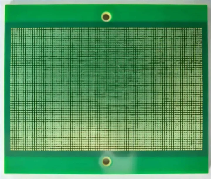
However, the company overcame all those difficulties and could manufacture the high-layer interposer PCB shown below.
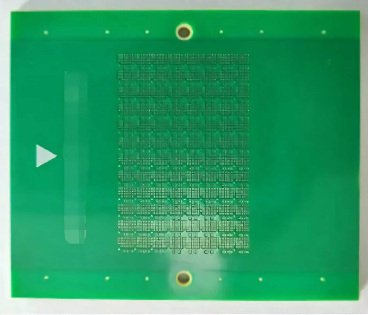
Feel free to contact PCBWay, if you have any requirements for high-layer, high-order interposer PCB manufacturing services. They can provide an online quote for PCBs with up to 60 layers.

This account is for paid-for, sponsored posts. We do not collect any commission on sales, and content is usually provided by the advertisers themselves, although we sometimes write it for our clients.
Support CNX Software! Donate via cryptocurrencies, become a Patron on Patreon, or purchase goods on Amazon or Aliexpress


