FLIP_C3 ESP32-C3 board takes up to 60V DC input, ships with ESPHome firmware

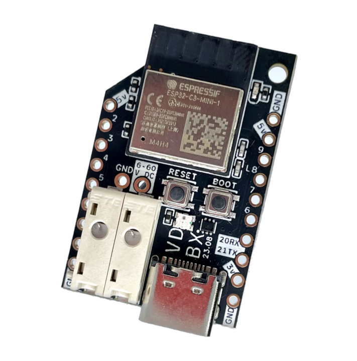
Voidbox FLIP_C3 is an open-source hardware board powered by an ESP32-C3 WiFi & BLE microcontroller that takes up to 60V DC power input feeding a 5V/2A DC-DC step-down converter and flashed with ESPHome firmware by default for Home Assistant support.

flip c3 board front

The board incorporates a push-in spring release connector which means stranded (ferrules or tinning are suggested) and solid wires can be used in deploying the device in off-grid/battery-powered systems with up to 16s LiFePO4 delivering 48V through the 6-60V input port on the ESP32-C3 board. The onboard WS2812B LED can be used as a null pixel/level shifter for longer strings of addressable pixels.

The ESP32-C3 – due to its support for Wi-Fi and BLE connectivity – is a popular SoC for IoT solutions and powers home and industrial automation devices such as NanoCell v2.1, Spark Analyzer, LOLIN C3 Pico, and the LILYGO T-RSC3.

It is built for home automation applications and comes with ESPHome preloaded for easy integration with Home Assistant. However, it is easy to install other firmware such as Tasmota and WLED on the device via USB-C and over-the-air updates.

FLIP_C3 specifications:

  • Microcontroller – ESP32-C3 RISC-V MCU @ 160 MHz, with Wi-Fi and BLE 5 connectivity pre-loaded with ESPHome for Home Assistant
  • USB – USB-C for alternative power and programming; reverse current protection from DC input via diode
  • Expansion
    • I2C and UART on JST SH1.0 4-pin connectors compatible with Stemma QT and Qwiic modules
    • 9-pin + 10-pin headers with GPIO, I2C, UART, 5V,. 3.3V, and GND
  • Onboard LEDs
    • WS2812B RGB LED with D-Out sent to L8 on pin header
    • Status LED
  • Buttons – Boot, Reset
  • Onboard 5V/2A buck converter
    • Power – Up to 10W (with cooling)
    • Tolerant up to 50V DC for direct connection
    • 60V absolute max (with pre-charge resistor)
  • Push-in, spring terminal for DC input
    • Solid: 24 – 16 AWG
    • Stranded: 22 – 18 AWG
    • 2x2P 2/54 pass-through power header for stacking
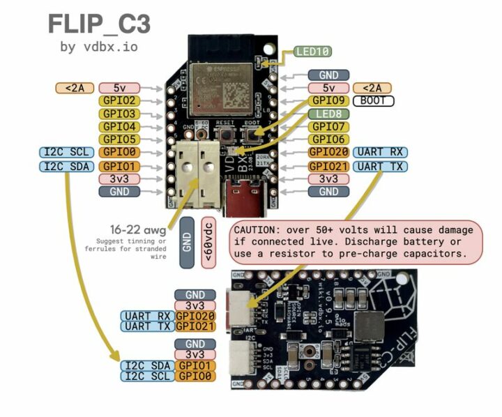
flip c3 pinoutTypical applications of the FLIP_C3 board include:

  • Deploying short runs of addressable LEDs using level-shifted output from WS2182B, and
  • Reading Daly BMS data via UART and using the onboard buck converter to supply power from a 14s Li-ion or 16s LiFePo4 pack.

The board is open-source and hardware files are hosted on OSHWLab. A 3D DIN rail mount can be downloaded from printables.

The FLIP_C3 is available on Amazon and Tindie for $20. More information about the product and other VoidBox projects is available on the Voidbox wiki page.

Share this:

Support CNX Software! Donate via cryptocurrencies, become a Patron on Patreon, or purchase goods on Amazon or Aliexpress

Radxa Orion O6 Armv9 mini-ITX motherboard
Subscribe
Notify of
guest
The comment form collects your name, email and content to allow us keep track of the comments placed on the website. Please read and accept our website Terms and Privacy Policy to post a comment.
7 Comments
oldest
newest
Per
Per
7 months ago

It is in the right direction but article is a bit misleading.
It allows for continuous 50V operation and can surge 60V spikes.
In a nominal 48V battery system we see continuous 57V or so at charging… so this would be fried then.
Would really like true nominal 48V devices so waiting for their next gen then😊

Chloe
Chloe
7 months ago

Actually, it’s 60v tolerant stable. The issue is my lack of addition of a TVS diode for the higher transients from connecting ~51-60v – it works fine with 48v batteries if discharged below about 51v before direct connection. Future versions will fix this issue, but it should be an easy mod on existing boards that I’m currently testing and will document.

itchy n scratchy
itchy n scratchy
7 months ago

Tinning of stranded wires for push-in terminals is usually a good plan for wire breaks.
Actually we use stranded wires mostly with non push-in spring terminals, but where push-ins are given we also use them without ferrules: the trick is just to press the ejection “buttons” while inserting. This keeps the strands flexible and not prone to breaking when exposed to vibrations. If push-in functionality is a must have feature best is to use ferrules with a plastic collar, but keep in mind you can’t use the full range of cross sections when using ferrules, but mostly a non issue.

Chloe
Chloe
7 months ago

There was certainly a trade-off when selecting this style of connector and we’re just passing thru the datasheet’s specs alongside my own interactions with them. I def prefer ferrules and they should be used, but in a pinch you can tin some stranded.

Stefan Brüns
Stefan Brüns
7 months ago

The PCB layout is a prime example for things you should not do: Place the switching regulator next to your antenna Place the switching regulator diode next to the inductor (good), but route the shortest GND return path halfway accross the board Ignore the documented antenna keep out area Document the boot strap pins (IO2, IO8, IO9) in the schematic, but then leave out the required pull up resistors Also, don’t know why the switching regulator is set to 5.5 V, a dropout voltage of 2.2V for the linear regulator makes is run quite hot. The LMR16020 should be good… Read more »

Chloe
Chloe
7 months ago

Yes, I knew going into this that I was going to be breaking some “rules” but it certainly works, I do all the QC myself, and I’ve been running about 15 of them in my own bus conversion that I live in. You are wrong about the keep-out zone tho… it’s purely the antenna area that needs to be avoided which I do. Also all my grounds go straight into the two internal pours and the path length is negligible. IDK what you’re asking for in terms of pull-up documentation, could you elaborate? I’m also not sure where you’re getting… Read more »

Stefan Brüns
Stefan Brüns
7 months ago

I believe “it works”, I am just saying the design has several faults. Does you QC include EMI measurements? Probably not. Re. keepout area, I am not wrong. Read the design guidelines again: no PCB under the antenna, and no PCB left and right of it (at least 15mm, preferably more). No parts next to the antenna. IO2 should have a weak pullup, read the complete bootstrap section of the C3 design guidelines again. The loop area of the switcher is far larger than necessary. Follow the layout example in the datasheet. Read up about minimizing loop area for switching… Read more »

Boardcon Rockchip RK3588S SBC with 8K, WiFI 6, 4G LTE, NVME SSD, HDMI 2.1...