JLCPCB, arguably the most popular and best PCB manufacturer in the community, has now started to offer a flex PCB manufacturing service with a special price starting at $15 and up to $54 coupon codes for new users.
A flex PCB, also called flexible PCB or flexible printed circuit (FPC), is made by creating copper traces on a polyester or polyimide film and can used to fit into electronic products in the consumer, communication, medical, automotive, aviation, and military industries. Its main benefits are its flexibility so a flex PCB can arbitrarily be bent and moved replacing regular cables, especially on moving parts, and its size and light weight that allows them to be integrated with high reliability into products with a small form factor.
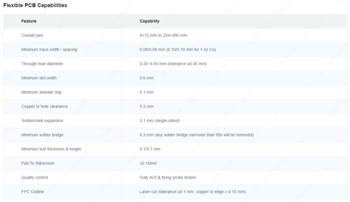
JLCPCB supports flex PCBs from 8x12mm to 234×490 in size with the full JLCPCB flex PCB capabilities shown in the table below.
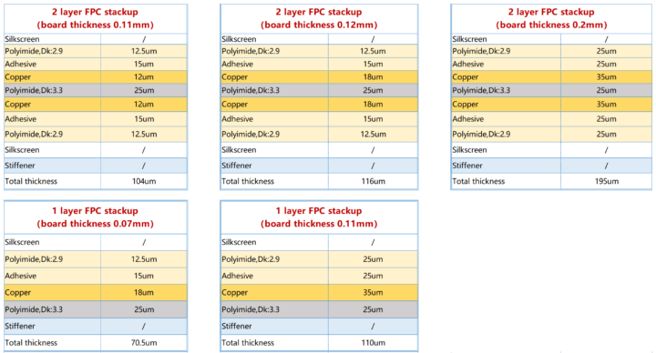
Hardware engineers can design flexible PCBs with one or two layers with a thickness from 0.07 to 0.12mm, and using materials such as Polyimide and copper. JLCPCB also says they can manufacture multi-layered Flex PCBs with three or more layers to allow more complex wiring.
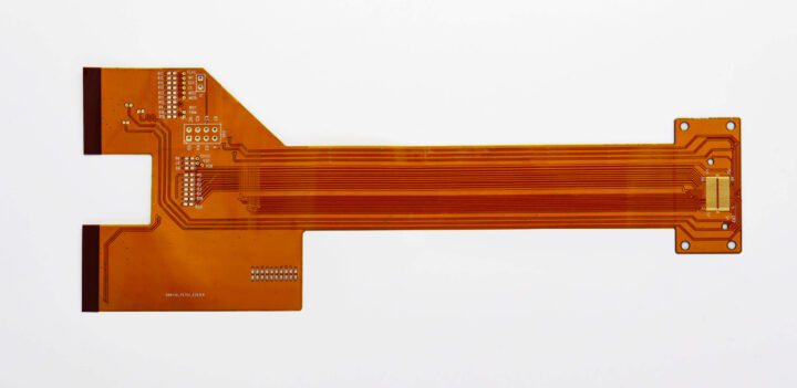
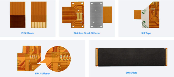
Flex PCB usually comes with a rigid part – called a PCB stiffener – to facilitate the insertion into a connector or mounting usually made of FR4, Polyimide, aluminum, or stainless steel. Here’s an example of a flex PCB manufactured by JLCPCB with a PI (Polyimide) stiffener.
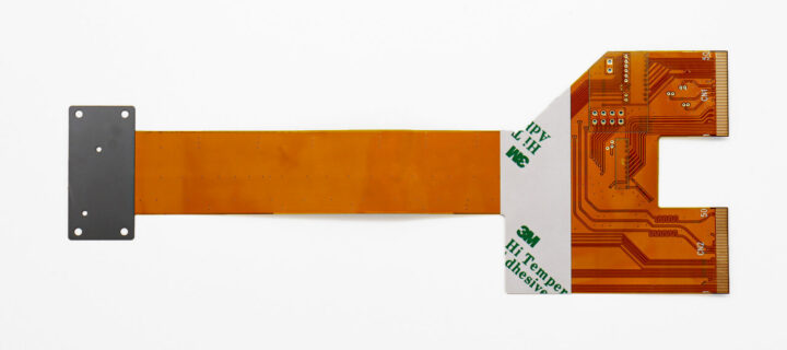
The flex PCB below is even more complex with a stainless steel stiffener (left), an FR4 stiffener (right), and a 3M tape stiffener (middle right).
JLCPCB provides some recommendations when designing and ordering Flex PCBs:
- Silkscreen text which overlaps ENIG pads will be made as hollow cut-outs in the pad if you select adhesiveless electro-deposited copper as the base conductor with ENIG surface finish.
- Exposed connector pads should be ≥ 0.2 mm from the FPC’s edge as areas closer than this limit will be removed.
- Stiffeners and EMI shields are optional additions that should be described by an individual Gerber layer or a separate CAD drawing and annotated with the material and thickness required
JLCPCB’s popularity drives its large-scale production capabilities and further enables the company to lower its manufacturing and shipping prices, even for flex PCB manufacturing services.
JLC is constructing a one-stop industrial electronic platform, realizing digital PCBA processing by merging EDA, PCB, components sourcing, and PCBA services. With increased investment in innovation and digital systems, they have been rapidly developing and have established themselves as a leading worldwide PCB&PCBA manufacturer, offering quick manufacturing of high-reliability and cost-effective products.

This account is for paid-for, sponsored posts. We do not collect any commission on sales, and content is usually provided by the advertisers themselves, although we sometimes write it for our clients.
Support CNX Software! Donate via cryptocurrencies, become a Patron on Patreon, or purchase goods on Amazon or Aliexpress
