Samsung Electronics has unveiled its first Universal Flash Storage (UFS) 4.0 solution based on the company’s 7th-generation V-NAND and a proprietary controller allowing speeds of up to 23.2 gigabits per second (Gbps) per lane or double the previous UFS 3.1 solutions.
In more practical terms, Samsung UFS 4.0 storage will deliver a sequential read speed of up to 4,200 MB/s and a sequential write speed of 2,800 MB/s, corresponding to about 2x and 1.6x faster speeds over UFS 3.1 storage.
Samsung also claims that power efficiency has been enhanced with a sequential read speed of up to 6.0 MB/s per milliampere (mA), or about a 46-percent improvement over UFS 3.1. An advanced Replay Protected Memory Block (RPMB) is integrated into the chip to store important personal data that can only be read or written through authenticated access, and whose design is said to be 1.8 times more efficient.
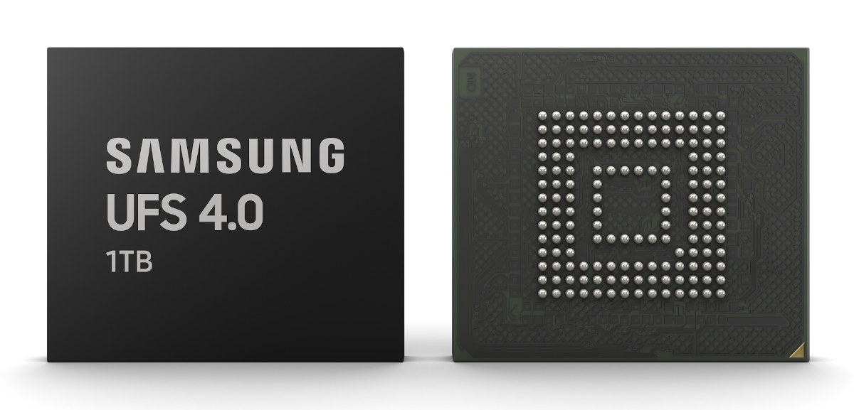
Samsung UFS 4.0 storage will be offered in a 13 x 11 x 1mm package and be found in 5G smartphones, as well as automotive and AR/VR applications. Mass production is expected to start in Q3 2022 and be sold in various capacities up to 1TB. More details may be found in the announcement. I was also going to redirect readers to JEDEC website for the UFS 4.0 specification, but it does seem to have been published just yet.
Via Liliputing

Jean-Luc started CNX Software in 2010 as a part-time endeavor, before quitting his job as a software engineering manager, and starting to write daily news, and reviews full time later in 2011.
Support CNX Software! Donate via cryptocurrencies, become a Patron on Patreon, or purchase goods on Amazon or Aliexpress