We covered Xassette-Asterisk open source-hardware Allwinner D1s RISC-V Linux SBC last October. But it will most likely never be mass-manufactured since SdtElectronics, the designer, has no resources and time for production. So I thought I should give it a try, and I managed to get 10 boards manufactured and assembled.
Time for a little disclaimer. While the post is not sponsored in the sense I did not get paid for it, NextPCB agreed to cover all costs, aka sponsor, and manufacture ten boards. Today, I’ll report my experience manufacturing an open-source hardware board, but I had no time to check whether any of the boards worked.
Manufacturing timeline
Since I did not want to go through the whole process of ordering the PCB, purchasing the components, and soldering each board individually, I opted for NextPCB’s PCB manufacturing and assembly services. Here’s the detailed timeline:
- November 9 – Ordered 10 boards on NextPCB using Gerber files and BoM on Github.
- November 10
- Received an (automatic?) email saying my order failed verification
- Received an email from my assigned support contact (Betty) telling me drilling data was missing, and asking for further clarification about some items in the BoM.
- Sent drill data after generating it from KiCAD using those instructions. Asked SdtElectronics to help me with the BoM issue.
- November 11
- Got a reply from SdtElectronics and sent the updated BoM with clarifications
- NextPCB still had some small issues with the BoM (LED color, Allwinner D1s purchase link, etc…)
- Since some of the components are optional, I could handle that myself without bothering SdtElectronics, and provided instructions
- Clarification about the order (9 fully assembled board, 1 bare PCB) as I made some mistakes while ordering online.
- November 12 – More questions about BoM, mostly asking about confirmation about connectors, Crystal part, etc… But I missed that email and did not reply…
- November 16
- Asking me again about BoM, and this time I did reply.
- Received an email saying my order had been verified successfully
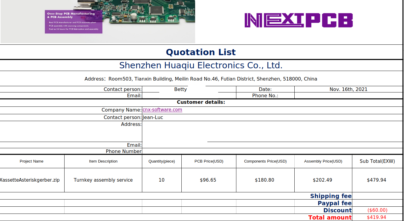
- Received a quotation (To this point, I don’t think the person in charge knew I would not pay for it…)

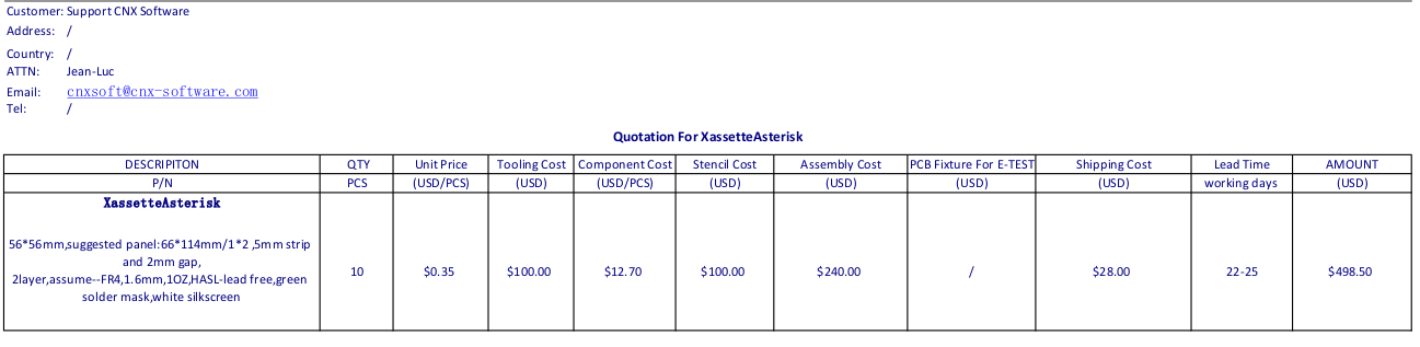
$419.94 in total before shipping, or about $41.90 per board. If that board was mass-manufactured it would cost closer to $10 per unit, and that’s why companies are doing crowdfunding… - Sometimes companies contact CNX Software before reading the “About” page, and another company asked me if I had any PCBs to manufacture, so I received a quotation from another company (Note that’s for 10 fully assembled boards, instead of 9+1).

$498.20 including shipping. That’s quite similar to the NextPCB quotation, so $40-$50 per assembled board should be the expected cost for such a small order. I did not manage to get free samples from this manufacturer…
- November 18
- Received an email from Betty asking if I checked the quotation
- I replied I was not going to pay! 😮
- November 19
- Received an email saying the payment was successful!
- Received an “urgent” email telling me I had selected the “castellated holes” process when uploading the PCB files (oops, my bad), and was asked for the pick and place file for assembly. I followed some instructions on Seeed Studio to generate the file from KiCAD.

- November 22, 2021
- Received Working Gerber (also in PDF format) for verification. I was also told they made some changes: ” for the position by arrow indicated, it can not be made as solder mask bridge, so our engineer suggests that help you connect the pads together(whole opening), is ok for you?”

- I contacted SdtElectronics again to check the Gerber and get feedback about the “solder mask bridge” since I did not clearly understand it:
I assume gaps between pads at some positions are too small to make solder mask upon. As long as the manufacturer will take care of the soldering that would not be a problem, otherwise the absence of solder mask may cause difficulty to soldering (by hand).
- I also gave the go-ahead with production
- Received Working Gerber (also in PDF format) for verification. I was also told they made some changes: ” for the position by arrow indicated, it can not be made as solder mask bridge, so our engineer suggests that help you connect the pads together(whole opening), is ok for you?”
- November 23
- Received an email saying fabrication will start, that components are sourced and everything is going, and not to worry… I also got a further explanation about the solder mask bridge “issue”.
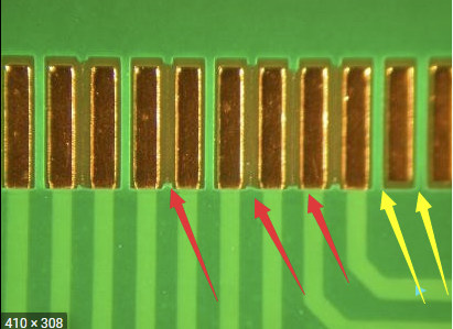
Please check the picture, the position by yellow arrow indicated is made as solder mask bridge, the position by red arrow indicated is made as “connect the pads together”, also you mean “no solder mask”.
 Now that’s super clear.
- Received an email saying fabrication will start, that components are sourced and everything is going, and not to worry… I also got a further explanation about the solder mask bridge “issue”.
- November 30 – Email update informing me the PCB fabrication had been finished, the components were in transit, and should be received next week. Plus details about the next steps:
- Count the components first, compare the pads on board.
- Start the assembly production if no any issues need to confirm.
- Send you the sample board photos to confirm.
- Continue to the rest production and ship out the boards soon.
- December 7 – Urgent email asking me for the Pick and place file. I thought I had already sent those on November 19, but sent them again.
- December 10
- Received photos of the first sample for checking. I was also informed about some problems with the design:
… the parts circled by red line, the pads are a little smaller, they may be pulled off in Reflow soldering process, we will help you repair them manually before shipment, but also please improve your this design in future.

Most of the capacitors are not soldered because they fell off after reflow soldering due to the small pads. For sample quantities, the manufacturer can rework the board and manually fix the issues, but the design should be modified for mass production, and I was told they would do so. - Apart from that, the board looked fine to me, but SdtElectronics kindly provided feedback again:
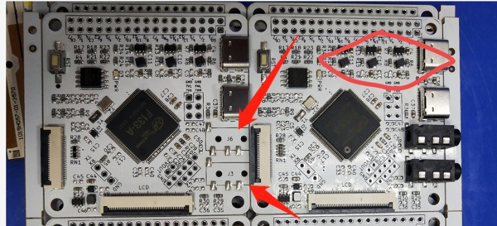
I did find some issues from the pics you uploaded. R21, R18 and R17,
R14R4 are jumpers for boot media selection and they must NOT be soldered simultaneously. I have mentioned this in notes of README, as well as the commented BOM list. Should a card was used as the only boot media, all these 4 resistors can be removed. Same reason for R33 and R32. They are jumpers and only one of them should be soldered (R32 for most LCD panels).About the skew components (3 inductors in your pics), I have also experienced this when soldering by hot plate (they were right, melted solder paste pulled components off) and I have to adjust them manually. This would not be a problem as long as two pads of the inductor are not shorted.
- Received photos of the first sample for checking. I was also informed about some problems with the design:
- December 13
- Sent feedback to NextPCB
- Received photos of updated PCB

I focused on the removal of R4, R18, R17, R21, and R33 (on the back, not visible on photo above) and that was fine to me. The capacitors were still not soldered, and I thought this would be done manually later (rookie mistake! as we’ll see later), so I gave the go-ahead to complete production.
- December 17
- Received an email from Betty saying production was complete, and the board would be shipped today
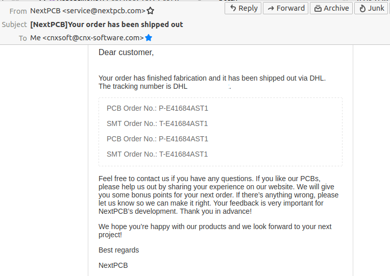
- Receiving an automatically generated email with DHL tracking number

- December 22 – Received the board in Thailand
- December 23 evening – Boards in CNXSoft hands!
So far, I was quite pleased with the way it was handled. It took around 6 weeks from order to delivery. Another person also built the board by himself and apparently did so in about two weeks.
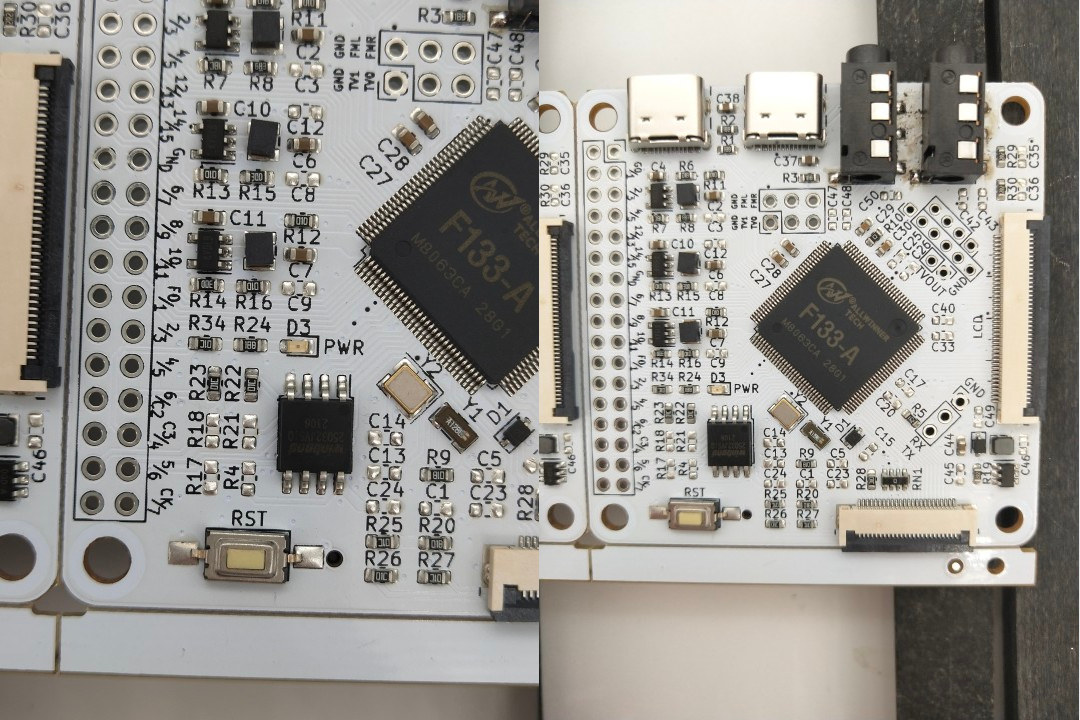
Checking out Xassette-Asterisk boards
So let’s see what we’ve got…
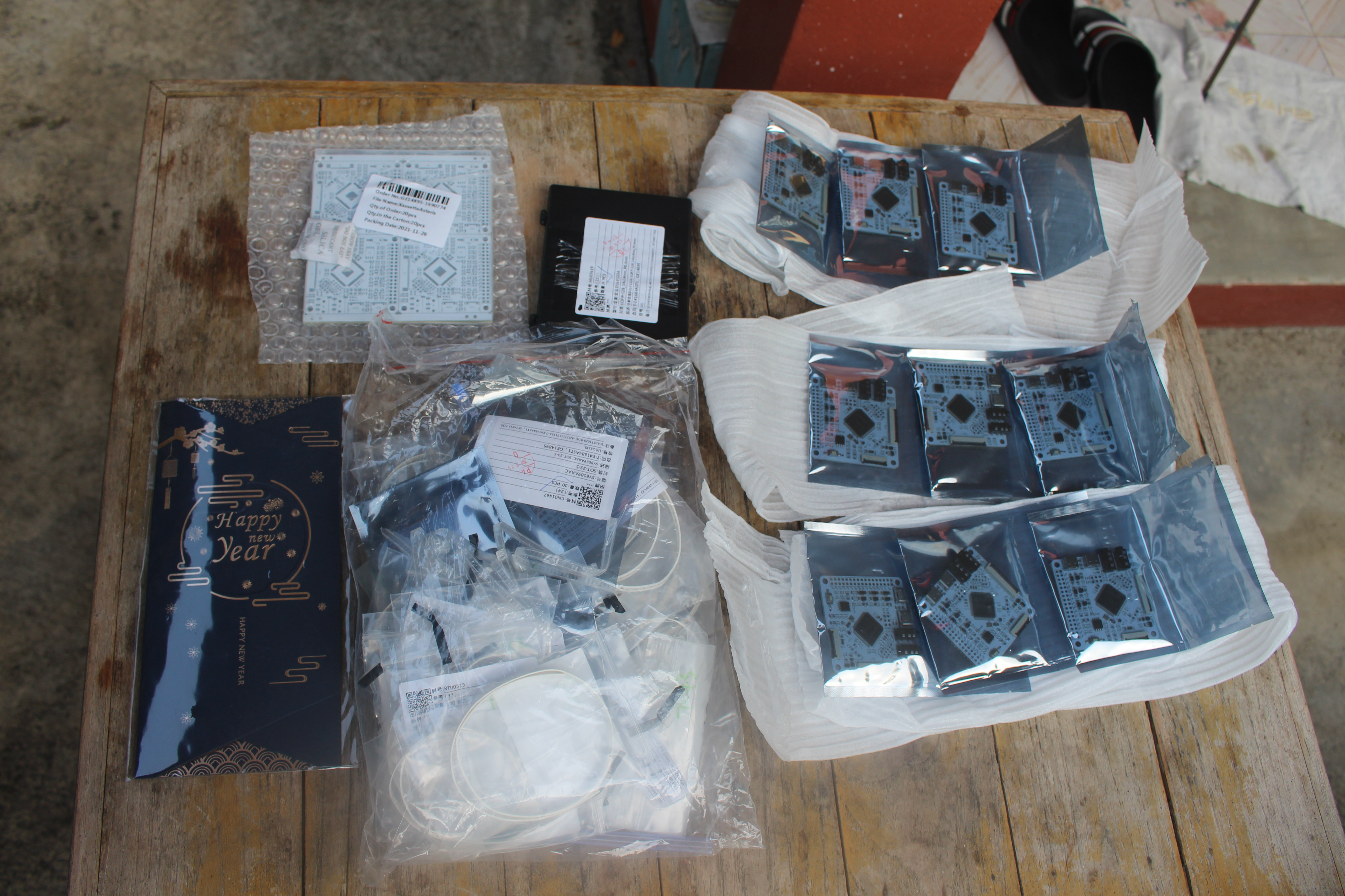
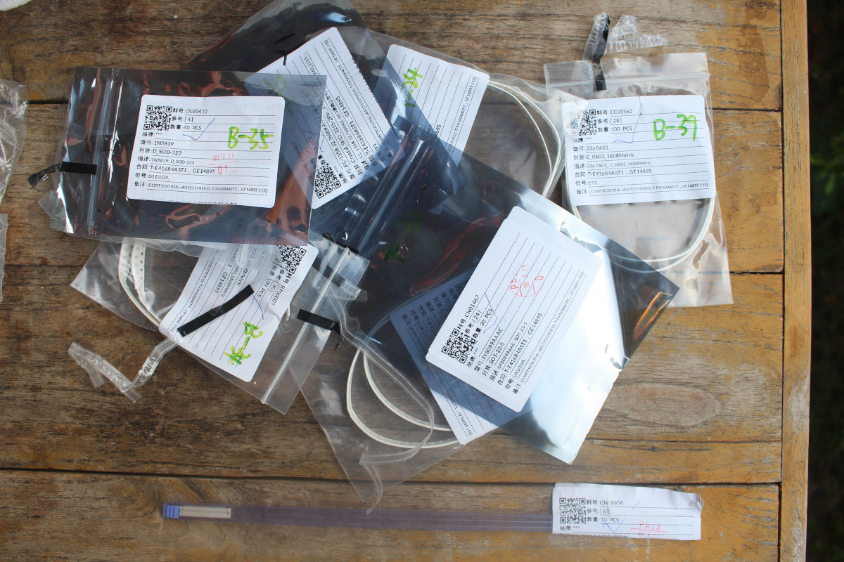
I only expected 9 assembled and one non-assembled board, but I got a bit more than expected including one bag with “garbage” as jokingly described by my girlfriend. That bag contains unused components. That’s because suppliers won’t just sell bags with 9 components (except for the processor see black box), and will ship the components in varying quantities of 10, 30, 40, or even 100 pieces as illustrated by the photo below.
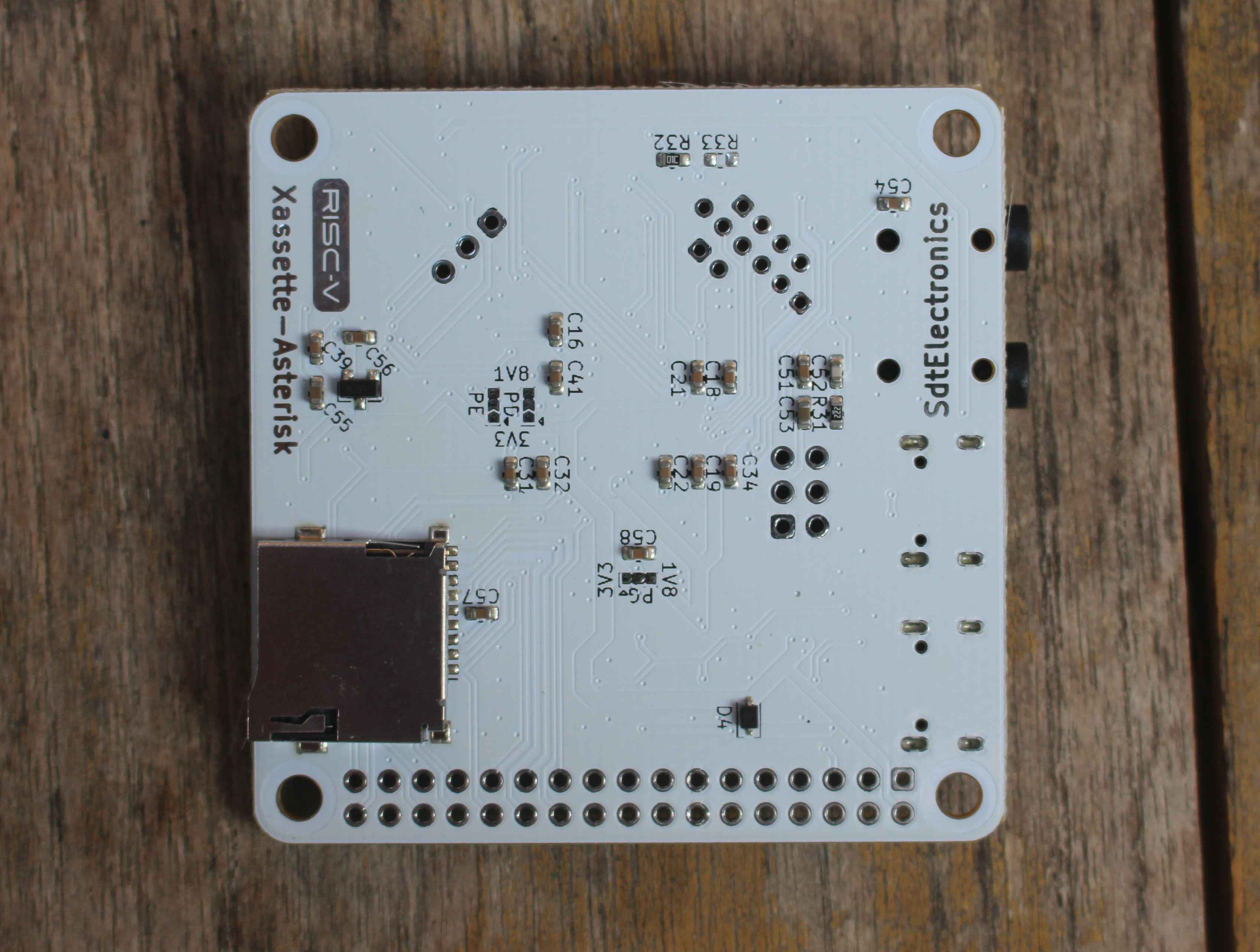
Time to have a look at the bare PCBs. I received two panels of four boards each.
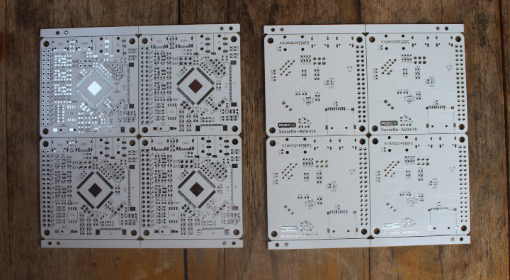
Higher resolution shots…
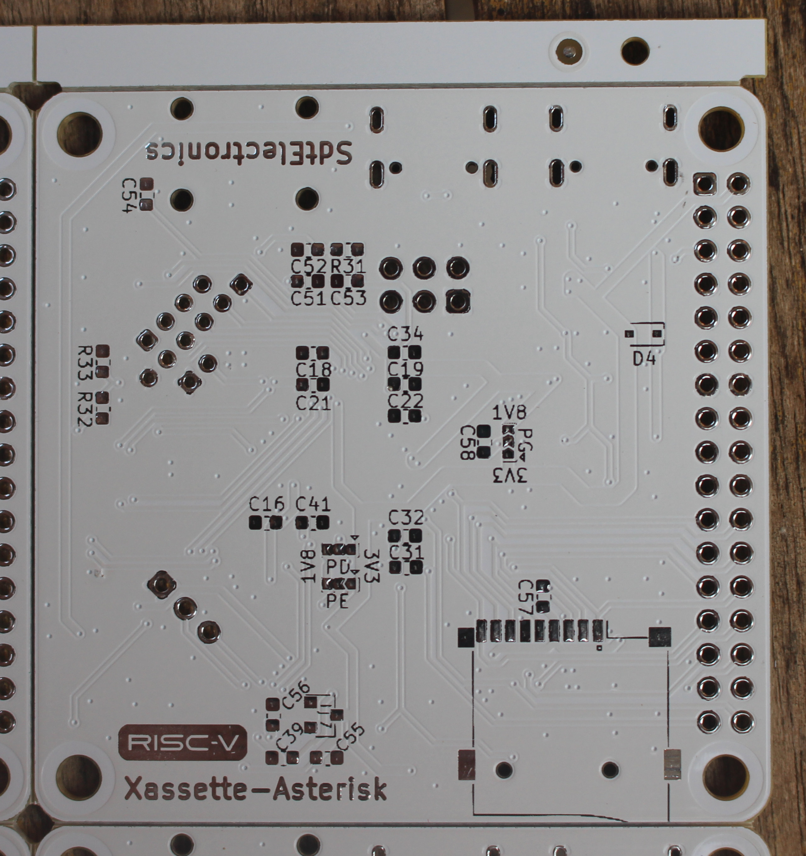
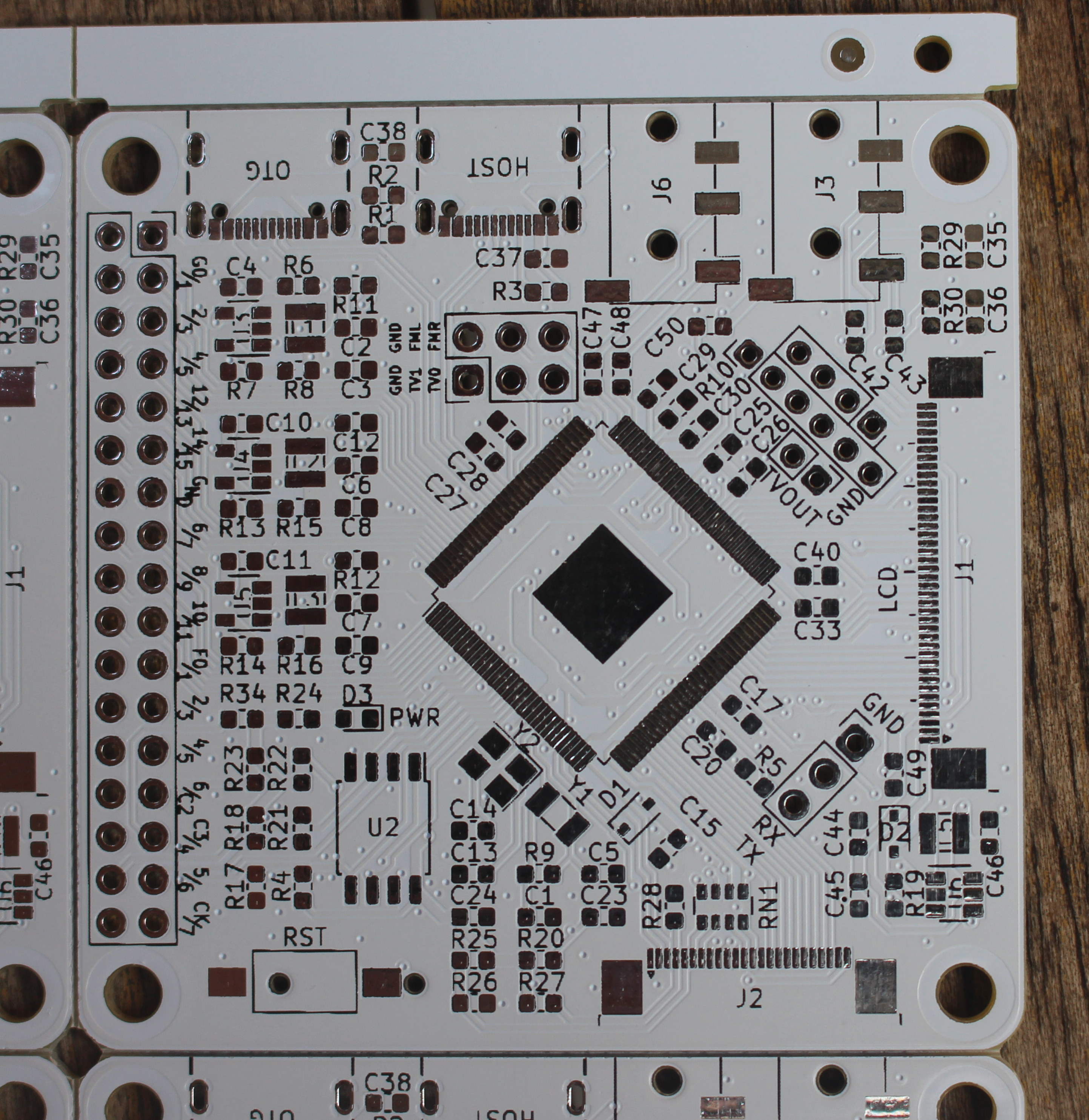
and now for the fully assembled board…
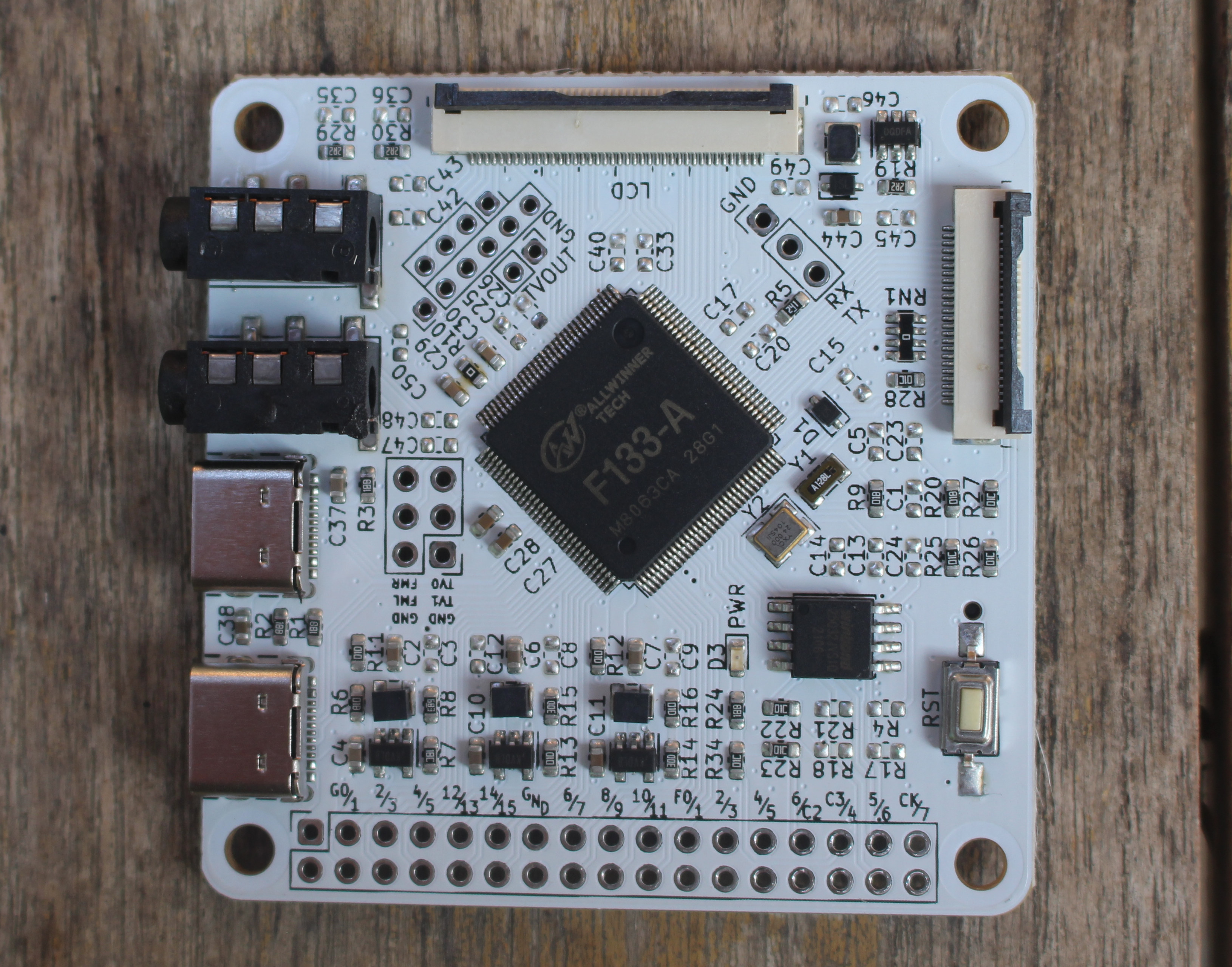
and in the sun…
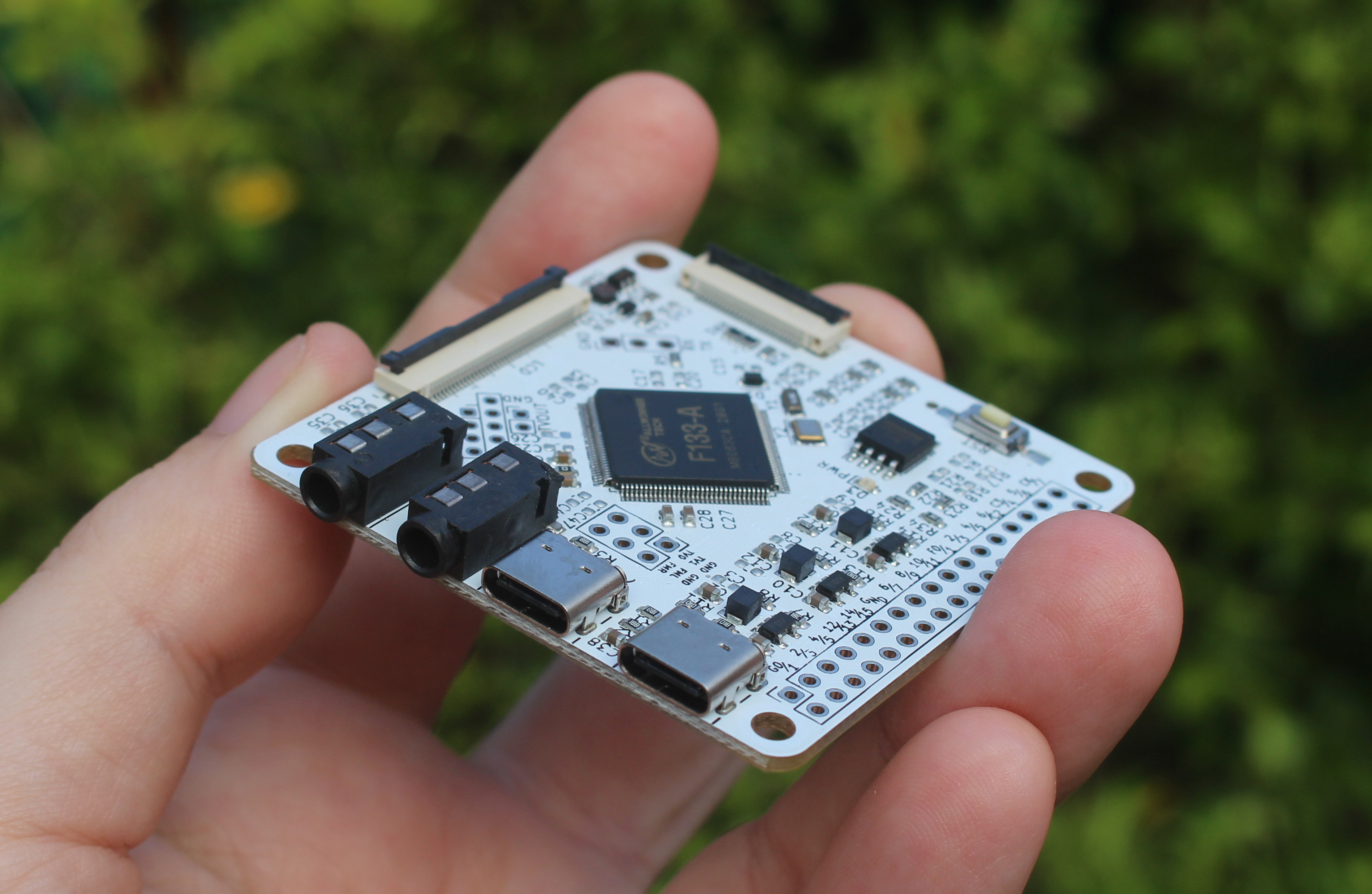
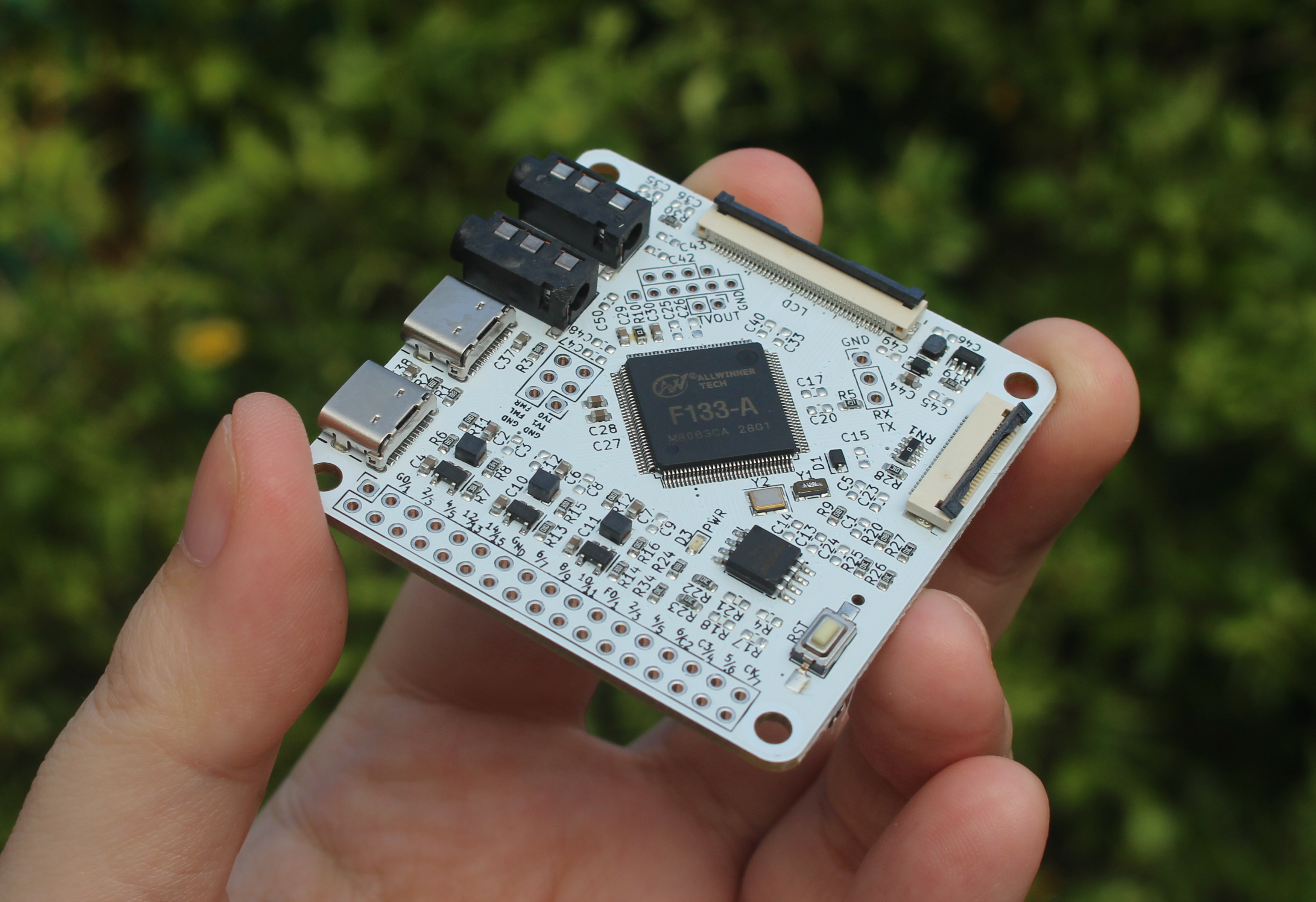
It all looks good to me except the capacitors that fell off during reflow soldering were not soldered manually, so I’d have some work to do before testing the board.
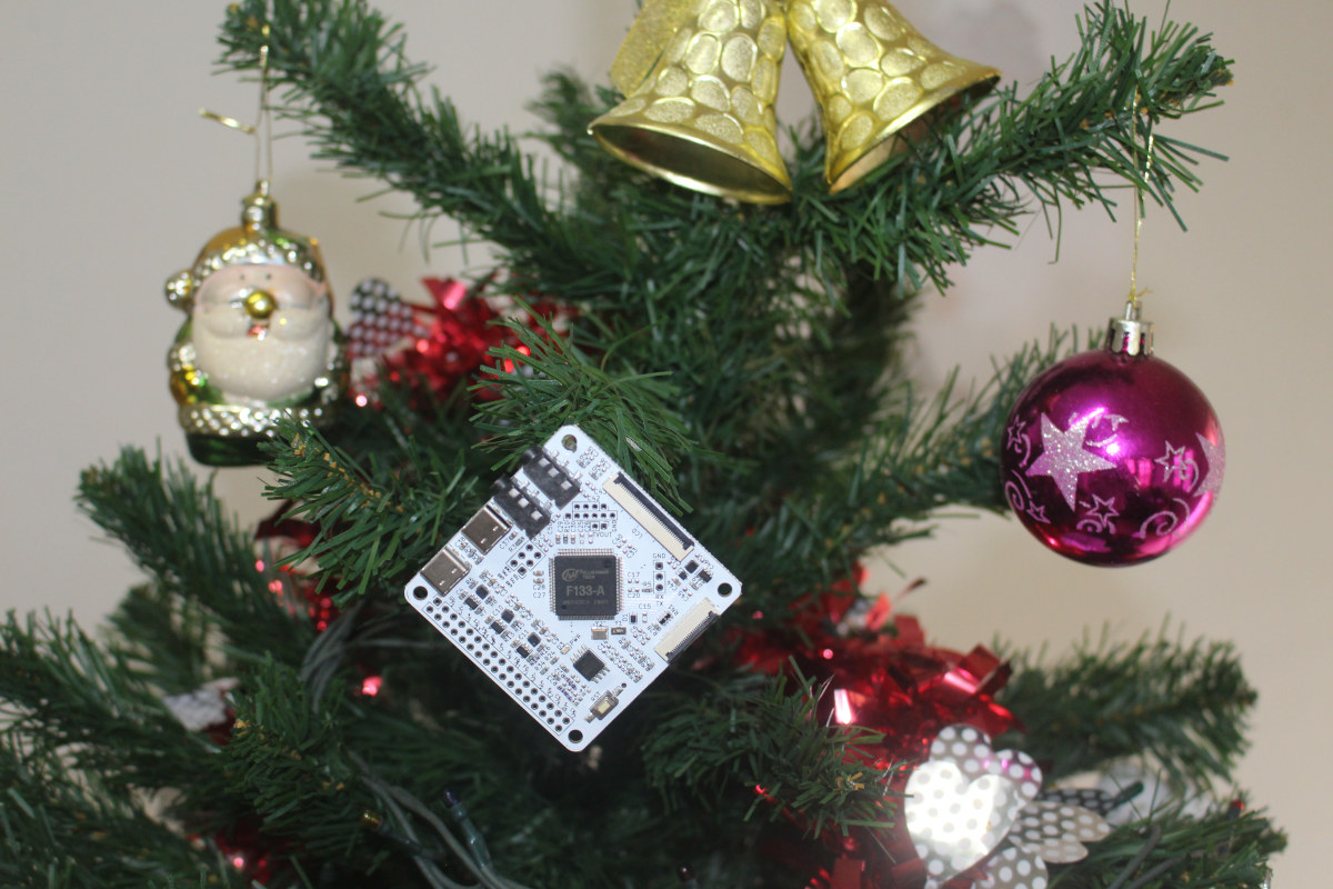
This will take a while since I won’t have access to a soldering iron for several weeks. If the boards don’t end up working, they make great Christmas tree ornaments!
If you’d just like to play with an Allwinner D1s or F133-A, I’d recommend waiting for the MangoPi MQ board that should start selling very soon. But if you like a challenge with some soldering and board bring up, I’m giving away 6 pieces of the assembled boards, [Update: all boards have been taken] and the two bare PCB panels. I’d just ask $7 for registered mail (count 2 to 4 weeks). Only one board or panel per person, and I’ll include some components bag as well (after keeping some capacitors for myself). Since I don’t expect many takers for a board that may or may not work, you can just reach out through the contact form if you are interested.

Jean-Luc started CNX Software in 2010 as a part-time endeavor, before quitting his job as a software engineering manager, and starting to write daily news, and reviews full time later in 2011.
Support CNX Software! Donate via cryptocurrencies, become a Patron on Patreon, or purchase goods on Amazon or Aliexpress