Texas Instruments unveiled their first 64-bit processor in 2018 with TI AM654 “Keystone III” quad-core Arm Cortex-A53 + dual lockstep Cortex-R5F processor designed for general embedded and industrial applications.
The company is now working on a more powerful processor with J721E SoC with Cortex-A72 cores belonging to the K3 Multicore SoC architecture platform appearing in TI Linux git repository. Ti J721E is a monster of an SoC, not necessarily in terms of CPU processing power, but it has an amazing amount of features and peripherals.
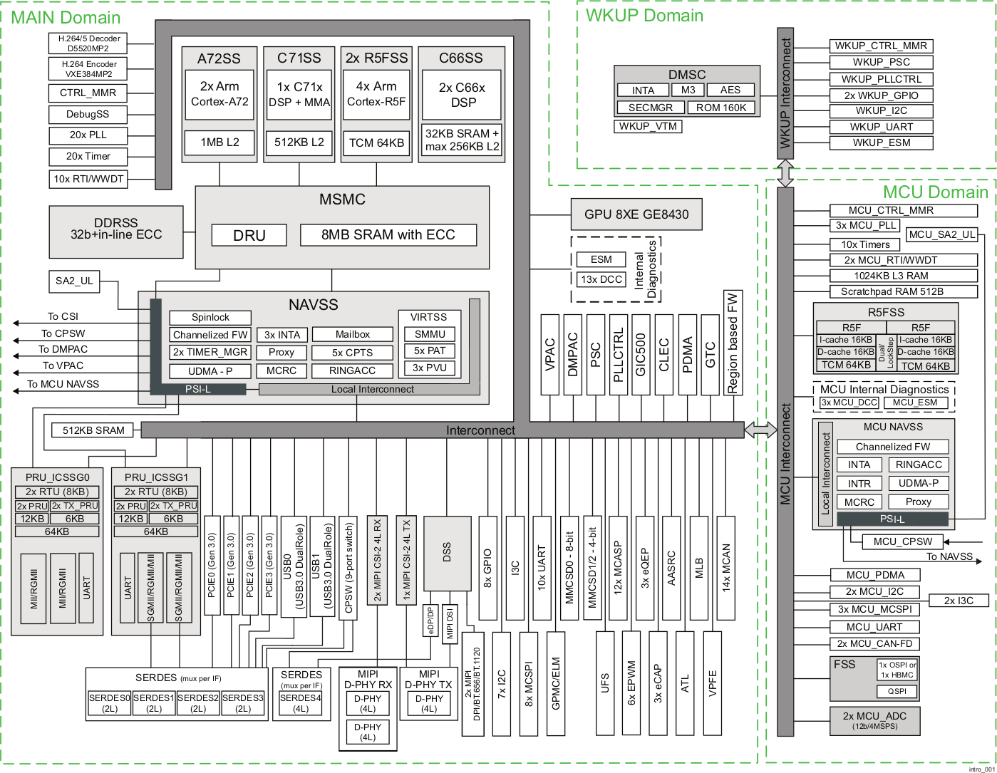
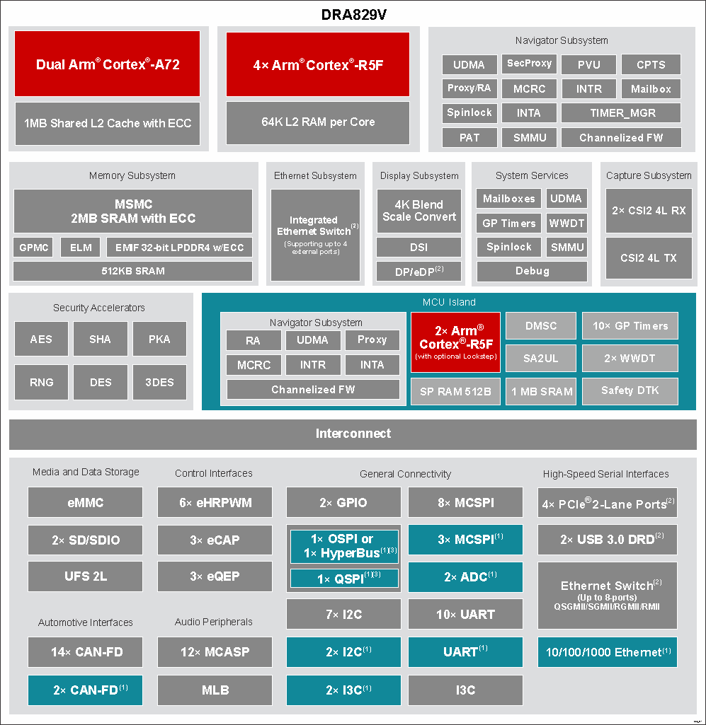
I’m not going to list all specifications of this monster SoC, and we’ll do with J721E highlights instead:
- CPU
- Dual Cortex-A72 up to 2.0 GHz in a single cluster
- Up to three clusters of lockstep capable dual Cortex-R5F MCUs @ 1.0 GHz
- AI Accelerator / DSP
- Deep-learning Matrix Multiply Accelerator (MMA) @ up to 1.0 GHz (8 TOPS for 8-bit inference)
- C7x floating-point Vector DSP @ up to 1.0 GHz (80 GFLOPS)
- Up to two TMS320C66x floating-point DSPs @ up to 1.35 GHz (40 GFLOPS)
- Multimedia
- GPU – Imagination PowerVR Rogue 8XE GE8430 GPU
- Vision Processing Accelerator (VPAC) with image signal processor
- Depth and Motion Processing Accelerator (DMPAC)
- 1x dual-core multi-standard HD Video Decoder
- 1x dual-core multi-standard HD Video Encoder
- Memory I/F –
- Storage I/F – 1x Octal SPI (OSPI), GPMC for 8-/16-bit parallel NOR or NAND flash, 3x MMC/SD controllers, 1x UFS interface
- Two Navigator Subsystems (NAVSS) for data movement and control
- System MMU (SMMU) Version 3.0 and advanced virtualization capabilities.
- Peripherals
- Display – 1x eDP/DP, 1x MIPI DSI, and up to 2x DPI interfaces.
- Camera – 2x 4-lane MIPI CSI 2.0 Rx (camera receiver), 1x 4-lane MIPI CSI 2.0 Tx (camera transmitter)
- Audio – 12x MCASP (Multichannel Audio Serial Port) supporting up to 16 channels
- Networking
- Up to 2x Gigabit Industrial Communication Subsystems (ICSSG), each with dual PRUs and dual RTUs
- Integrated Ethernet switch supporting up to a total of 8 external ports in addition to legacy Ethernet switch of up to 2 ports.
- Up to 4 PCIe GEN3 controllers
- 2x USB 3.0 Dual-role device subsystems
- 16 MCANs, 12 McASP, eMMC and SD, UFS, OSPI/HyperBus memory controller, QSPI,
- 3x I3C, 12x I2C, 11x master/slave MCSPI, 12x UART, 10x GPIO modules
- Security
- 2x hardware accelerator blocks containing AES/DES/SHA/MD5 called SA2UL management
- Secure Boot Management
- Public Key Accelerator (PKA) for large vector math operation
- Trusted Execution Environment (TEE)
- Secure storage support
- On-the-fly encryption and authentication support for OSPI interface
- Manufacturing Process – 16-nm FinFET technology
- Package – 24 x 24 mm, 0.8-mm pitch, 827-pin FCBGA (ALF), enables IPC class 3 PCB routing
The device is partitioned into three functional domains, each containing specific processing cores and peripherals:
- Wake-up (WKUP) domain
- Microcontroller (MCU) domain with one of the dual Cortex-R5 cluster
- MAIN domain
This domain fragmentation enables the device to achieve lower power dissipation profiles by allowing the power supplies to unused domains to be completely turned off and allows efficient addressing of safety requirements. Note the MCU and WKUP domains are combined into a common MCU/WKUP domain in J721E family of devices, but there are still separated in the documentation for compatibility with other K3 platform SoC’s.
If I understand correctly J721E will not be a processor per se, but it represents a family of processors that encompass the upcoming AM752x, DRA829, and TDA4VM SoCs. The AM752x SoC is targeted at the generic embedded systems market, industrial control, defense, and avionics while the DRA829 and TDA4VM SoCs are targeted at automotive applications with ASIL-B/C certification/requirements in mind.
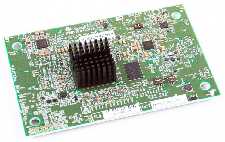
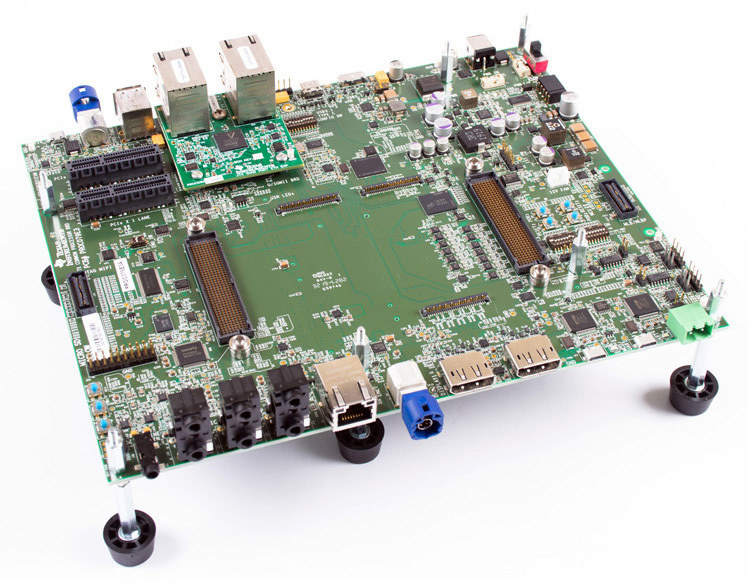
There’s no specific product page for J721E right now, but you’ll get plenty of information in the 15,556-page long technical reference manual, and more details in DRA829V product page. Everything is still in “preview”, but pre-production samples of DRA829V are available for $129.01 (sample price) or $97.00 for 1k orders, as well as DRA829Vx evaluation module with a choice of common, infotainment, and gateway baseboards. The devkits appear to be available now for $1,900 and up.
Thanks to Nobe for the tip.

Jean-Luc started CNX Software in 2010 as a part-time endeavor, before quitting his job as a software engineering manager, and starting to write daily news, and reviews full time later in 2011.
Support CNX Software! Donate via cryptocurrencies, become a Patron on Patreon, or purchase goods on Amazon or Aliexpress