CNXSoft: This is a guest post by Marcel Ziswiler, Platform Manager – Embedded Linux, Toradex and Leonardo Graboski Veiga, Technical Marketing Engineer, Toradex related to Marcel’s upcoming talk “Wear Estimation for Devices with eMMC Flash Memory” at the Embedded Linux Conference 2019 later this month.
Flash memory has been an important topic in embedded systems for decades. It allows for drastic improvements to the size and robustness of electronic devices compared to other storage technologies. Other benefits of flash storage include a lack of moving parts and reduced power consumption. However, the challenges that come with flash memory are not as widely publicized in consumer electronics. Among them are limited durability and greater software complexity.

As shown in Figure 1, flash memory is everywhere in our daily lives, ranging from devices used specifically to store data, such as thumb drives, SD cards and SSDs, to other consumer electronics that use it internally, like smartphones, Wi-Fi modems and smart light bulbs.
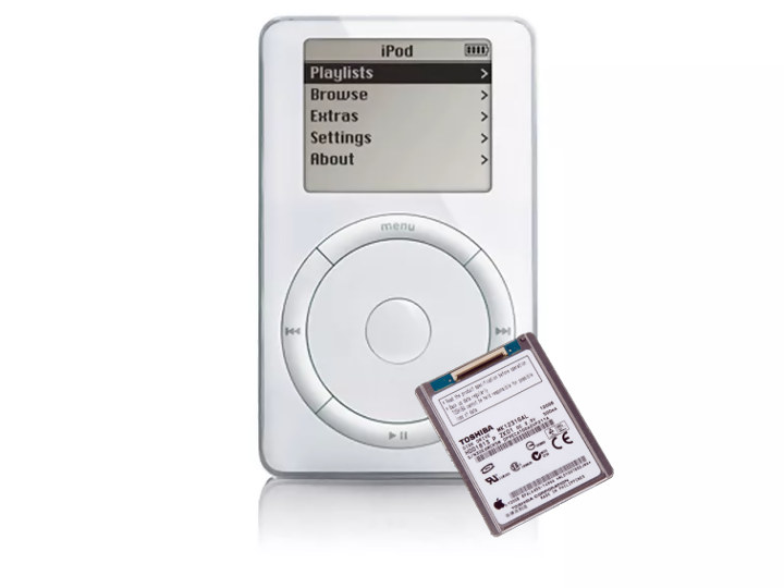
An iconic counterexample is the first model of the iPod, released in 2001. It used a spinning hard disk in order to provide a high storage capacity (for its time — 5 or 10 GB). A study found, however, that the perceived failure rate of models with an HDD was greater than 20%, compared to a rate of less than 10% on models equipped with flash memory. Due to the sensitive moving parts they contain, spinning disks don’t handle mechanical shock very well. This plays a significant part in the failure rate of portable devices equipped with magnetic storage.
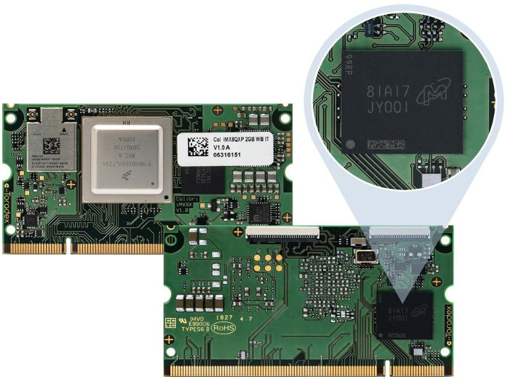
When it comes to embedded systems, flash is the non-volatile memory of choice. In embedded Linux systems, it is a common practice to use integrated circuits (ICs) in system on modules (SoMs) and single board computers (SBCs), as they are often more resistant to data corruption than several models of micro SD card. They are also more robust when environmental vibration is a decisive factor. Examples of SoMs that use integrated flash memory include the Apalis and Colibri families from Toradex. In Figure 3, you can see a zoomed-in view of the Colibri iMX8X module, equipped with an eMMC from Micron:
The goal of this article is to present an overview of how to design more reliable embedded systems by taking advantage of both open-source and proprietary software to measure and estimate eMMC wear. This is motivated by (e.g.) the ever-increasing need for IoT gateways and data loggers, as well as a desire to keep redundant data on site for either increased reliability or intermittent connectivity reasons. For practical details of implementation, Toradex SoMs equipped with Micron eMMCs are used to exemplify how a wear monitoring and estimation solution — the Flash Analytics Tool — can be brought to life.
This article also includes a broad technology overview and some implementation specifics. This information may not be new to you, so feel free to skip sections if you already have the requisite knowledge or as you deem fit.
Technology Overview
Before going any further, it’s worth noting that flash memory is a topic so broad that even an article devoted to addressing how it works would still not provide a sufficiently comprehensive overview of it. The following paragraphs are meant only as background to better understand how to estimate eMMC wear.
While this article only presents the essentials for understanding wear estimation, a wide variety of literature on flash storage is available on the Internet. Toradex, for instance, has a blog, a webinar archive and a range of articles on its developer website. Wikipedia’s article on flash memory also has literally more than one hundred references to other resources.
NOR and NAND
Flash memory is a broad term, and there are several combinations of technologies that together form final flash products with specific characteristics. An initial distinction can be made by segregating flash storage into two types: NOR and NAND. These are named after how the technology operates at the transistor level to store bits, resembling NOR and NAND logic gates.
While NOR has simpler principles of operation and higher reliability, it often requires a higher pin count and has a lower density of storage per unit area of silicon than NAND, which impacts its size and cost. For these reasons, NOR is often used only in specific applications considered critical even for industrial-grade, highly reliable embedded systems. You can learn more about this topic in the NOR | /NAND Flash Guide from Micron (PDF). You can see a summary of NOR and NAND technologies in the context of storage density and capacity in Figure 4, taken from the guide referred to in this paragraph:
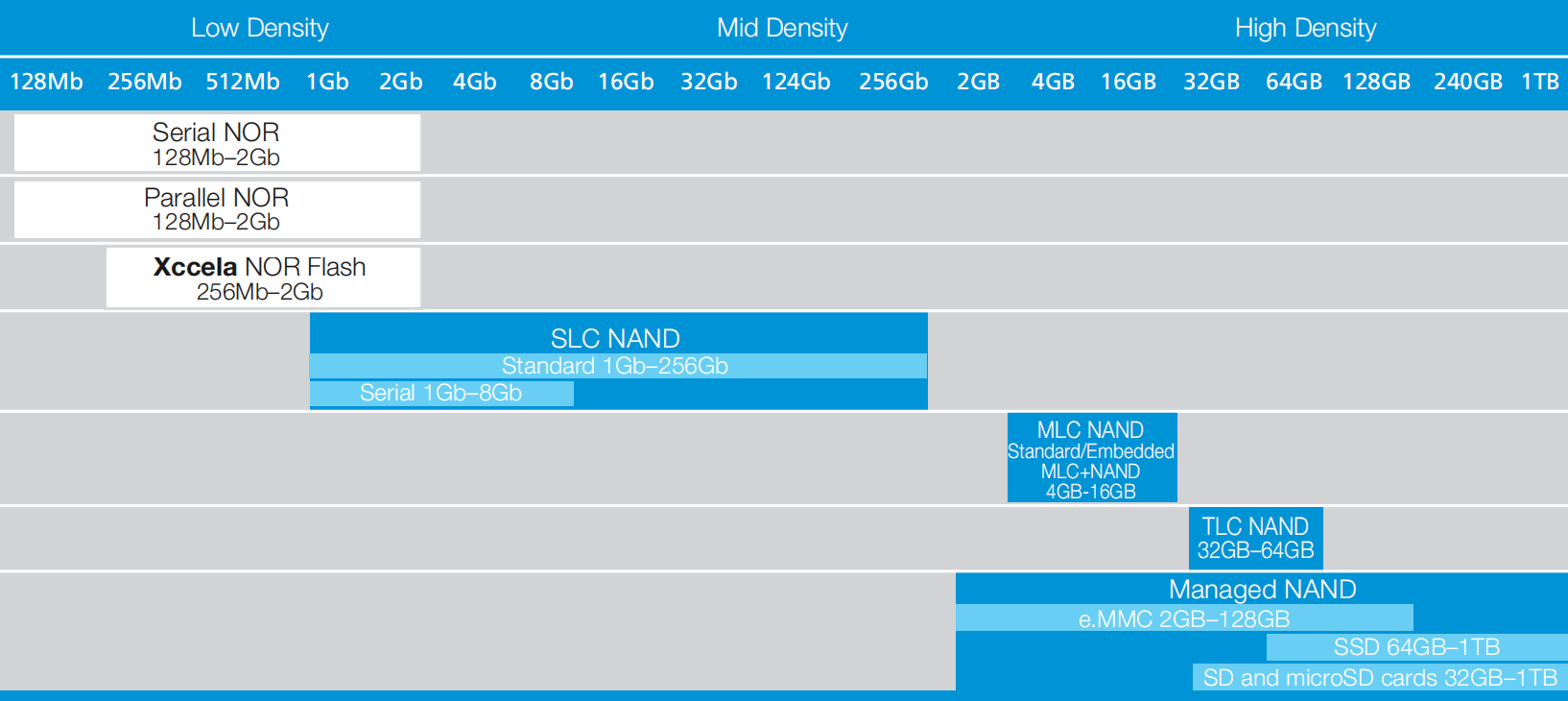
As you can see, Micron eMMCs are exclusively NAND devices in the MLC and TLC ranges, which we will discuss in more detail. Since Toradex SoMs use eMMCs in the 4GB to 16GB range, we can infer that they use MLC devices. This will also be addressed later in this article.
NAND Structure
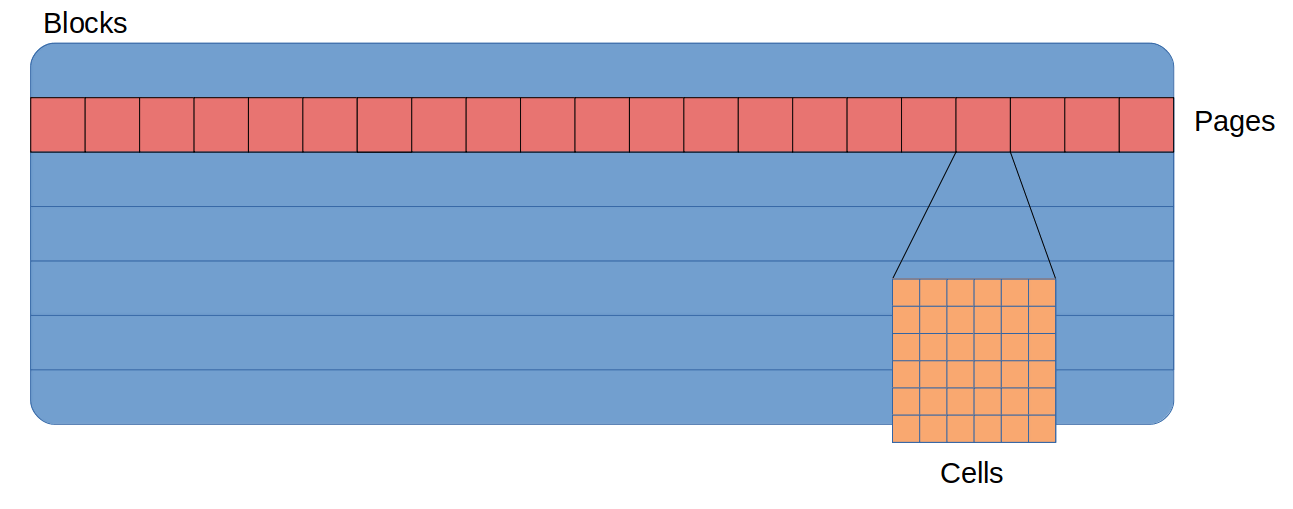
A raw NAND flash device can be broken up into three distinct parts.
- Cell: The smallest entity. A cell stores data at the bit level and is not directly addressable by the device controlling the NAND storage.
- Page: The smallest array of cells that can be addressed for read and program operations. A program operation consists of “flipping” bits from the value 1 to the value 0. Page sizes are in the kilobyte range; e.g., 4 KB.
- Block: The smallest array of pages that can be addressed for erase operations. A block is also known as an eraseblock in some contexts, such as the Linux MTD stack. An erase operation consists of returning bits with a value of 0 to a value of 1. Block sizes are in the megabyte range; e.g., 4 MB. Erase operations are much slower than program or read operations executed on pages.
- Erase operations wears out flash storage over time.
- When a block is no longer usable for storing data, it is labeled a bad block.
The most important information from the points above is that blocks wear as they are erased. Thus, for our purposes, we are most interested in the block erase count; that is, the number of times each block has been erased.
NAND SLC and MLC
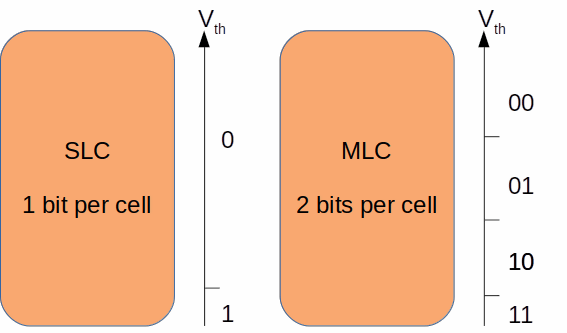
A cell, as the smallest entity, stores bits. How many bits are actually stored per cell depends on the voltage level thresholds it can hold and distinguish during a read operation. There are various designations for flash memory that indicate how many bits the cells can store.
- SLC: single-level cell, stores 1 bit per cell
- pSLC: MLC operating in SLC mode, stores 1 bit per cell
- MLC: multi-level cell, stores 2 bits per cell
- TLC: triple-level cell, stores 3 bits per cell
- QLC: quad-level cell, stores 4 bits per cell
There is a trade-off between density and cost versus reliability and lifespan, summarized in Table 1.
|
NAND Cell Technology |
Density (bits per cell) |
Cost |
Reliability |
Lifespan |
|
SLC |
1 |
Highest |
Highest |
Highest |
|
pSLC |
1 |
Average |
High |
High |
|
MLC |
2 |
Average |
High |
Average |
|
TLC |
3 |
Low |
Low |
Low |
|
QLC |
4 |
Lowest |
Lowest |
Lowest |
Table 1: NAND cell technologies comparison
The Figure 6 helps to visualize how SLC and MLC store bits:
The pSLC (“pseudo-SLC”) improves the speed of operations and lifetime of an MLC device, at the expense of reducing its capacity by half. The lifetime doesn’t match that of a true SLC, but it is greatly increased. Pseudo-SLC should not be confused with Fast Mode, which makes an MLC device faster but does not improve its lifetime:
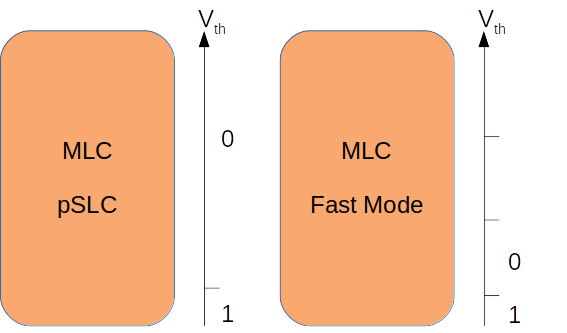
Understanding if blocks are configured as MLC or pSLC is important in determining the lifespan of the device as we collect the bad block count over time.
For an eMMC that uses MLC technology, depending on the trace width of the silicon, a block lasts for 3000 to 10,000 erase cycles on average. The lifetime for pSLC is increased by a factor greater than 2 compared to MLC; therefore, pSLC is preferred over Fast Mode or over-provisioning (i.e., using flash memory with double the capacity to make it last twice as long). It can be difficult to find erase cycle count and trace width values in manufacturers’ publicly available documentation, so benchmarking the devices themselves may be a solution.
ECC
We briefly went over the fact that blocks wear out and become bad. When they are healthy, though, not everything is necessarily perfect. Bits may be randomly flipped, corrupting the stored data. This is where the ECC, or Error Correction Code algorithm, steps in to correct the flipped bits.
With time, the probability of a bit flip in a block increases. When it becomes too great, the block is marked bad. It may happen that a block goes bad prematurely, and a storage device may be shipped from the factory with some bad blocks. Manufacturers often include spare blocks to replace these, such that they do not immediately affect the usable storage capacity.
Write Amplification
Write amplification is, in a few words, the copying of data from one block to another, be it for the purpose of updating that data, wear leveling or any other reason.
Wear leveling and Garbage Collection
If one always uses the same physical pages and blocks, such as when updating a file, those blocks will become worn prematurely. In the worst-case scenario, the system may even stop working far before the flash memory’s end of life (EOL) if the NAND controller does not relocate data as those blocks become bad.
To prevent this from happening, a wear leveling algorithm ensures that blocks are always used evenly. To accomplish this, it moves data around. There are two types of wear leveling algorithms.
- Dynamic: Only data that is dynamic (i.e., updated over time) is moved around. Static data is kept in the blocks it was originally written to. This algorithm is simpler but does not use the entire capacity of a storage device. It is best employed when only a small percentage of the flash memory holds static data.
- Static: This algorithm purposefully moves static data around, wearing all blocks of the flash memory evenly. This is a more complex algorithm, but it extends the lifespan of a storage device by using all the available flash memory.
Garbage collection is the process of marking blocks as “dirty” when copying their data around for any reason, as opposed to simply erasing them right away. Dirty blocks are erased only at a later point in time, such as when the system is idle — but ahead of the time when the system will need those blocks again. Remember that erasing blocks is a slow operation, so proper garbage collection increases performance in some cases.
Figure 8 displays how the raw NAND management algorithms together can be seen as a controller that maps physical erase blocks (PEBs) to logical erase blocks (LEBs) and abstracts NAND-specific operations to simple “read” and “write” operations:
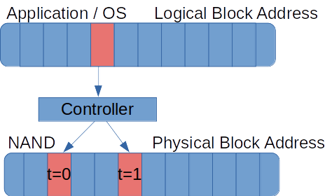
When a raw NAND chip is interfaced to a system that tries to implement a “dumb” controller to simply translate NAND program, read and erase operations to HDD-like read and write operations, it severely impacts the performance and lifespan of the flash memory. This is one of the reasons why the Linux MTD subsystem is almost always used by filesystems that are aware of raw NAND peculiarities — and possibly a layer in between, in the case of UBI and UBIFS — instead of filesystems that access block devices.
If you want to learn more about wear leveling, have a look at Micron’s TN-29-42: Wear-LevelingWear Leveling Techniques in NAND Flash Devices (PDF) and the “Wear leveling” article on Wikipedia (as well as its references, including some LWN.net articles). For garbage collection, read Micron’s TN-2960: Garbage Collection in Single-Level Cell NAND Flash Memory (PDF).
To understand the full implementation of abstraction layers between a raw NAND device and an application in detail, you can read the comprehensive MTD, UBI and UBIFS documentation. Of course, to learn the specifics of the implementation, you can have a look at the Linux kernel source- code as well.
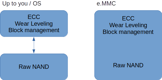
Despite all the complexity of raw NAND operations, which we nonetheless must know to some degree in order to create wear estimation models, a simple way to abstract this complexity away is to buy a NAND device with an integrated controller, also referred to as managed NAND. As far as integrated circuits go, common types include embedded USB, eMMC and UFS. Here, we’ll focus on eMMC.
A detailed look at eMMC Flash
One of the most popular high-capacity flash technologies used in industrial-grade embedded systems is eMMC (Embedded MultiMediaCard), which consists of a raw NAND die, usually MLC or TLC, and its accompanying NAND controller. It abstracts a large part of the management software stack from the underlying operating system. The eMMC standard is maintained by JEDEC and its base is accessible free of charge upon registration. The latest standard published until this article has been written is Embedded MultiMedia Card Electrical Standard 5.1 (PDF download after registration)
Since the controller provides a high-quality abstraction layer — provided that it comes from a reliable manufacturer — it’s safe to use a filesystem that is aware of block device operations as long as you take some precautions. In Toradex Embedded Linux BSPs, we use the EXT4 filesystem by default for computer on modules with eMMC flash. Figure 9 summarizes the differences between raw NAND and managed NAND with regards to the controller:
In the examples throughout this article, we consider a 4GB MLC eMMC with 1024 blocks, which in the real world could be (e.g.) the Micron MTFC4GACAJCN-1M-WT used in the latest revision of the Apalis iMX6Q 1GB SoM. We also assume an average block lifespan of 3000 erase cycles, which is just an educated guess. It was not taken from the aforementioned part number’s datasheet.
The challenges of using eMMCs lie in gathering details about the controller implementation and module lifespan that may or may not be publicly available. In addition, one may prefer to choose a manufacturer that provides a good proprietary health report. The eMMC standard reserves some registers for this purpose, but using them is optional. The eMMC chosen for the case study has a detailed health report, and detailed information about it can be taken from Micron’s TN-FC-32: e.MMC Device Health Report, available upon registration from the e.MMC Software section of Micron’s website. In this section of Micron’s website, you can also find the emmcparm tool which will be used later in this article, and the helpful TN-FC-25: Understanding Linux Driver Support for e.MMC.
Commands and Registers
The eMMC standard defines operations through a bus that contains power supply, CMD, DAT0-7 and CLK lines.
CMD is a serial channel and different CMD values represent different operations. After a command is sent from the host to the card, a response is issued from the card to the host through the same serial line. Related data is accessible through DAT lines. For curiosity’s sake, an illustration of a multiple-block read operation is provided in Figure 10. Luckily, all the tools we’ll use already implement and abstract eMMC communication for us.

The eMMC standard also defines registers with different sets of information, which are in turn accessible through specific CMD commands. Table 2 presents the eMMC registers:
|
Name |
Width (bytes) |
Description |
Implementation |
|
CID |
16 |
Device Identification number, an individual number for identification |
Mandatory |
|
RCA |
2 |
Relative Device Address, is the Device system address, dynamically assigned by the host during initialization. |
Mandatory |
|
DSR |
2 |
Driver Stage Register, to configure the Device’s output drivers. |
Optional |
|
CSD |
16 |
Device Specific Data, information about the Device operation conditions. |
Mandatory |
|
OCR |
4 |
Operation Conditions Register. Used by a special broadcast command to identify the voltage type of the Device. |
Mandatory |
|
EXT_CSD |
512 |
Extended Device Specific Data. Contains information about the Device capabilities and selected modes. Introduced in standard v4.0 |
Mandatory |
Table 2: e.MMC Registers (source: JEDEC Standard No. 84-B51, chapter 5.3, page 8)
The Extended Device Specific Data, formerly named Extended Card Specific Data, is where health reports are made available. It contains:
- a vendor proprietary health report, 32 bytes long
- device lifetime estimation type A, providing health status in increments of 10%
- This refers to SLC blocks in our eMMC.
- device life time estimation type B, providing health status in increments of 10%
- This refers to MLC blocks in our eMMC.
- pre-EOL info, reflecting device lifetime by average reserved blocks
- returns values normal, warning (80% of reserved blocks consumed) and urgent (90% of reserved blocks consumed)
A pertinent question: if that information is readily available, why not just use the data from the JEDEC standard?
- One reason is the fact that the health report was only introduced in revision 5.0 of the JEDEC standard.
- Another is the low resolution of the values (10% increments), which is bad for benchmarking applications that write small amounts of data. Very long run times would be required to obtain any useful information.
- In addition, a flash wear estimation tool that provides methods independent of specific technologies (i.e., also works for SD cards or raw flash on top of MTD) is more flexible.
Micron Proprietary Health Report
For this topic, we are (almost) outside the scope of the JEDEC standard. The only information we need to understand it is how to access this data. We need only know that we must use the General Command, viz. GEN_CMD or CMD56, as the entrance door to getting this data out of the silicon. The section Application-specific commands in the eMMC specification contains more details.
The next piece of information that we need is the vendor implementation of the health report. In our case, it is contained in Micron’s TN-FC-32: e.MMC Device Health Report, available in the e.MMC software area.
The following data can be obtained:
- Bad block counters and info: the factory bad block count, runtime bad block count and remaining spare block count. This also provides per-block information about failed page addresses and whether failures are on erase or program.
- Block erase counters: the minimum, maximum and average block erase counts among all blocks, as well as per-block erase counts.
- Block configuration: the physical address of each block and whether it is SLC or MLC.
To access each of these, CMD56 must be issued with a specific argument.
A Note on eMMC Support Over the Lifetime of an SoM
SoM manufacturers often have long-term availability policies, since they often target customers that benefit from this, such as industrial and medical users. For instance, Toradex guarantees more than 10 years of availability.
Often, the lifecycle of individual components is shorter than that of the SoM as a whole. Thus, new hardware revisions are released over time, communicated with Product Change Notifications (PCNs). This is one of the major advantages of using an SoM — it abstracts away the complexity of redesigns.
On the other hand, you may come up with hardware that has (e.g.) an eMMC that does not comply with the latest standards. That is another practical scenario where you want to have a wear estimation solution somehow detached from specific technologies or standards.
Flash Health
Flash health at any given point in time can be understood as the percentage of its capacity that has already been worn out. For simplicity’s sake, we will suppose that no blocks wear out at early stages, wear leveling is optimal and static, and there is no write amplification — that is, the ideal scenario.
The total endurance can be obtained in the total number of erases or the total amount of data that can be written to the device:
Where:
- E is the endurance expressed as the number of erase cycles (top) or bytes (bottom)
- B is a number of blocks
- Lavg is the average block lifespan expressed as a block erase count
- S is a block size in bytes
The total number of erase cycles, by definition, is more accurate because blocks wear from block erases. Therefore, the former method tends to be preferable to the latter.
In the example above, once 1,536,000 erases are evenly issued to blocks, or roughly 6 TB of data have been written to the device, it has reached 50% of its lifetime.
Monitoring Flash Health on Linux
To monitor the flash health parameters discussed in previous sections in Linux, one needs software that extracts meaningful information from the eMMC device. An open-source tool that can be used for this purpose is mmc-utils. It implements a good deal of the eMMC protocol, including reading data from the Extended Card-Specific Data (EXT_CSD) register and displaying it in a human-readable format. It includes the device lifespan as defined in the JEDEC eMMC 5.0 standard onwards. Let’s have a brief look at it by running the software without any parameters, which prints the help:
|
1 2 3 4 5 6 7 8 |
root@colibri-imx6:~# mmc Usage: mmc extcsd read <device> Print extcsd data from <device>. mmc extcsd dump <device> Print raw extcsd data from <device>. |
The output above focuses on the extcsd operations. If we execute the extcsd read command, we can obtain a range of information, including the JEDEC health status. Let’s see the header, or the first lines, of the output:
|
1 2 3 4 |
root@colibri-imx6-05097264:/app# mmc extcsd read /dev/mmcblk1 ============================================= Extended CSD rev 1.7 (MMC 5.0) ============================================= |
This confirms that we have an eMMC that adheres to the JEDEC 5.0 standard. Then, we can filter the output to get the health status as defined by JEDEC:
|
1 2 3 4 5 6 7 8 9 |
root@colibri-imx6:~# mmc extcsd read /dev/mmcblk1 | grep LIFE Device life time estimation type B [DEVICE_LIFE_TIME_EST_TYP_B: 0x01] Device life time estimation type A [DEVICE_LIFE_TIME_EST_TYP_A: 0x01] eMMC Life Time Estimation A [EXT_CSD_DEVICE_LIFE_TIME_EST_TYP_A]: 0x01 eMMC Life Time Estimation B [EXT_CSD_DEVICE_LIFE_TIME_EST_TYP_B]: 0x01 root@colibri-imx6-05097264:~# mmc extcsd read /dev/mmcblk1 | grep EOL Pre EOL information [PRE_EOL_INFO: 0x01] eMMC Pre EOL information [EXT_CSD_PRE_EOL_INFO]: 0x01 |
In the above example, we see that the health status is estimated between 0% and 10% of the device lifespan, with a normal pre-EOL status. Therefore, it is a new device. If we try to get the vendor’s proprietary health report, we find that it is not available from the upstream mmc-utils. Even the ChromiumOS downstream only displays zeroes:
|
1 2 3 4 5 |
root@colibri-imx6:~# mmc-cos extcsd read /dev/mmcblk1 | grep -i health Vendor proprietary health report: [VENDOR_PROPRIETARY_HEALTH_REPORT[301]]: 0x00 [VENDOR_PROPRIETARY_HEALTH_REPORT[300]]: 0x00 [VENDOR_PROPRIETARY_HEALTH_REPORT[299]]: 0x00 |
Nevertheless, one can always write some patches to try to extend the functionality of the tool. One example that could be used as a test might look like what is shown below. Notice that this code is not shown in full for clarity; e.g., validation is omitted:
|
1 2 3 4 5 6 7 8 9 10 11 12 13 14 15 16 17 |
/ Retrieve the erase count for each block // A two-step approach is needed (read number of tables and then read tables) int do_block_erase_info(int nargs, char **argv) { ret = CMD56_data_in(fd, cmd56_how_many_tables, data_in); printf("Block erase count\n"); printf("Block\tErase\n"); for(table_idx = 0; table_idx < how_many_tables; table_idx++){ ret = CMD56_data_in(fd, (table_idx * 256) + cmd56_retrieve_base, data_in); for(physical_block = 0; physical_block < 128; physical_block++){ printf("%d\t%d\n", (256*data_in[0+2*physical_block]) + data_in[1+2*physical_block], (256*data_in[256+2*physical_block]) + data_in[257+2*physical_block]); } } } |
Then we can have an application that retrieves the following data from Micron’s flash:
|
1 2 3 4 5 |
int do_bad_block_count(int nargs, char **argv); int do_bad_block_info(int nargs, char **argv); int do_block_erase_count(int nargs, char **argv); int do_block_erase_info(int nargs, char **argv); int do_block_addr_type_info(int nargs, char **argv); |
Another option is to use a vendor-specific tool, such as Micron’s emmcparm, that not only provides the consolidated lifespan report from JEDEC, but also the more granular parameters listed above and exemplified in the implementation proposal.
At the time of writing (August 2019), emmcparm has been periodically updated since version 2.6.0, released on May 27, 2016 (and possibly older versions no longer available from Micron) through version 4.4.0, released on June 5, 2019. The tool has several functions, of which the health status is one subset:
|
1 2 3 4 5 |
root@colibri-imx6:~# emmcparm_arm --spare_block --bad_block --erase_count --sect_count |
I/O Tracking
I/O tracking can be a useful indicator that flash is going to wear out quickly, as well as a debug indicator showing which applications are writing too much data. I/O tracking generates input data for a wear estimation model that doesn’t depend on JEDEC standards or eMMC vendor health reports. Therefore, it is a means of achieving the idea of a flexible tool that may be extended to various technologies, all of which use raw NAND as the storage technology.
The first step to implement a reliable I/O tracking mechanism is to build up some basic knowledge about how the Linux I/O stack works. At a very high level, usually what happens during application development is that you write some userspace code, and it performs file operations.
How the operations are done can vary depending on the library and language you are using, but at some point, there will be a transition from userspace to kernelspace. This is the point when the library’s functions will make system calls to the kernel. You can make a system call yourself, at the expense of abstraction and proneness to errors than a well-tested, mature library, such as the C standard libraries.
The Linux kernel then deals with that I/O through what is usually referred to as the I/O stack or storage stack. As its last step, it sends data to the device through a low-level device driver which, in the case of eMMC must be compliant with the JEDEC standard. At the highest level possible, Figure 11 identifies the stacks for raw NAND and eMMC devices
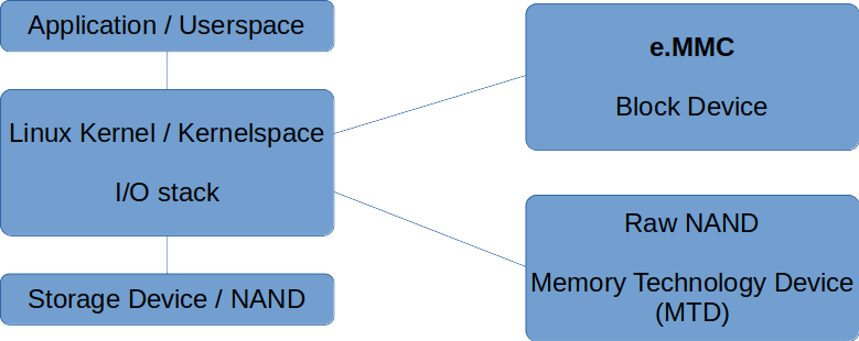
We can go through the kernel stack from top to bottom:
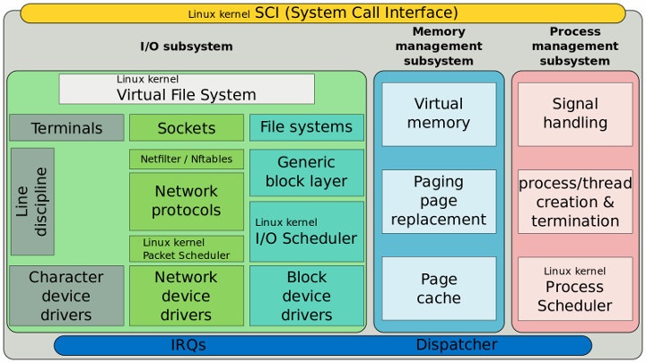
- The virtual file system is an abstraction layer for the userspace API.
- The file system itself implements a specific structure to define concepts related to files.
- A generic block layer, which often includes the I/O scheduler in the literature, is the place in the stack that handles all block I/Os (BIOs) and thus abstracts block devices for the file system, among other aspects.
- The I/O scheduler takes the queue of I/O requests and sends them to the block device driver according to a specific algorithm. It tries to maximize block I/O performance, and the choice of scheduler may affect latency, throughput and usage of the flash memory.
One may initially think that observing the number of writes to the flash over time, in order to obtain the write rate, could be done from userspace, and that would be good enough. However, the big problem with this approach is that it doesn’t result in an accurate measurement.
As shown in Figure 13, the Linux kernel is a complex system that implements layers of caches through its stack to prevent unneeded disk access. This is a concern because disk operations have always been slow; even with the advent of flash and its much faster operation, there is now the need to extend the lifetime of the storage device, and those caches and queues help with this:
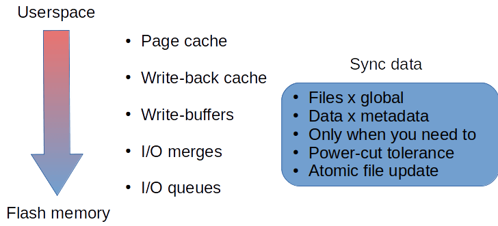
The Linux kernel implements a cache called the page cache that stands between the high-level VFS and the low-level file system. It is the kernel’s most popular caching system. It makes data readily available to userspace applications without having to go through the filesystem.
Deeper into the I/O stack, caching effects may occur due to I/O merges, to optimize the use of the storage hardware, and I/O queues that usually target throughput. As an example of merging I/O, there is the write-back mechanism that keeps data until absolutely necessary, thus preventing fragmentation and the use of fractional pages or blocks. Those mechanisms also make it hard to trace how much of a specific process’s writes are actually reaching flash memory.
As a side note on data sync, which may be critical for embedded system use cases (especially those without a back-up power supply) and which may affect the flash lifetime, care must be taken to sync only when data absolutely must be saved, even in the event of a power cut. A user pressing a “save” on a machine’s touchscreen panel is an example of one such occasion.
Measuring I/O Writes
The problem becomes more defined from our perspective of monitoring and accounting for all writes that actually reach flash memory:
- Where on the Linux stack are we guaranteed to be able to measure writes that actually reach flash memory?
- How do we measure this? (What tools can we use?)
Unlike health status measurements, which have a limited number of tools that may be used to gather data, the observability tools available for the Linux kernel stack are numerous. An example of this is shown in Figure 14, taken from Brendan Gregg’s blog. Brendan Gregg is one of the most knowledgeable people in the field of Linux performance monitoring.
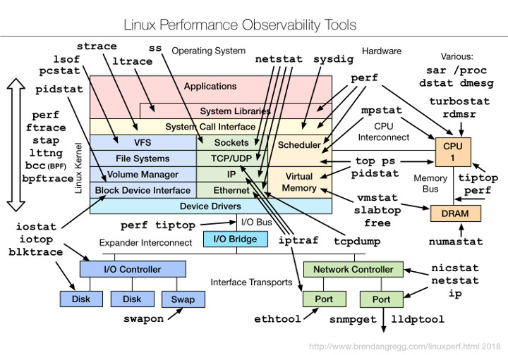
During the course of my research, I came across iotop to track user-space operations, and blktrace/blkparse to accurately track block-level I/O and what actually reaches flash memory as good candidates for the challenge. Since I’m not a kernel hacker and there is still so much room for research on the topic, I’m not implying in any way that those are the best or most optimized tools for the job. (For instance, perf trace and eBPF are also on my to-do list.) There is an interesting article on the subject named Linux block I/O tracing, as well as many other resources on the internet, including the Linux kernel documentation itself.
The importance of tracking I/O at the block level is accuracy, since it’s the only way to be sure that a write operation has actually reached flash memory instead of being flushed from cache or merged by a subsequent file system operation in the kernel. This is important, in turn, because what really must be accounted for are the number of times a block has been written to (erased, actually), and not just the actual amount of data that an application has tried to write.
Let’s briefly see in practice how we can use iotop and blktrace.
iotop conveniently has some options that help with this task, and it is very easy to collect and parse timestamps, write counts, and the processes responsible for these writes:
|
1 2 3 4 5 6 7 8 |
root@colibri-imx6:~# iotop –help Options: -o, --only only show processes or threads actually doing I/O -b, --batch non-interactive mode -a, --accumulated show accumulated I/O instead of bandwidth -k, --kilobytes use kilobytes instead of a human friendly unit -t, --time add a timestamp on each line (implies –batch) -q, --quiet suppress some lines of header (implies --batch) |
You can see an example below:
|
1 2 3 4 5 6 7 8 9 |
root@colibri-imx6:~# dd if=/dev/urandom bs=4k count=100000 | pv -L 25k > testfile root@colibri-imx6:~# iotop --only --batch --accumulated --kilobytes --time –quiet TIME TID PRIO USER DISK READ DISK WRITE SWAPIN IO COMMAND 2019-08-02 03:11:19 50 be/4 root 0.00 K 24.00 K -0.00 % -0.00 % pv -L 25k 2019-08-02 03:11:20 50 be/4 root 0.00 K 52.00 K -0.00 % -0.00 % pv -L 25k 2019-08-02 03:11:21 50 be/4 root 0.00 K 80.00 K -0.00 % -0.00 % pv -L 25k 2019-08-02 03:11:22 50 be/4 root 0.00 K 104.00 K -0.00 % -0.00 % pv -L 25k 2019-08-02 03:11:23 50 be/4 root 0.00 K 128.00 K -0.00 % -0.00 % pv -L 25k |
When it comes to blktrace, things are a bit more complicated. A good place to start looking at is the documentation. Running it in live mode without filters can present an overwhelming amount of output:
|
1 2 3 4 5 6 7 8 |
root@colibri-imx6:~# blktrace -o - /dev/mmcblk1 | blkparse -i - 179,0 0 26 0.000114661 304 A WS 4509800 + 8 <- (179,2) 4468840 179,0 0 27 0.000117328 304 Q WS 4509800 + 8 [jbd2/mmcblk1p2-] 179,0 0 28 0.000119661 304 M WS 4509800 + 8 [jbd2/mmcblk1p2-] 179,0 0 29 0.000127328 304 U N [jbd2/mmcblk1p2-] 1 179,0 0 30 0.000131661 304 I WS 4509736 + 72 [jbd2/mmcblk1p2-] 179,0 0 31 0.008860277 279 D WS 4509736 + 72 [kworker/0:3H] 179,0 0 32 0.012586780 279 C WS 4509736 + 72 [0] |
Luckily, filters are implemented in both blktrace and blkparse to ease the task. Table 3 lists them with brief descriptions:
| barrier | barrier attribute |
| complete | completed by driver |
| fs | FS requests |
| issue | issued to driver |
| pc | packet command events |
| queue | queue operations |
| read | read traces |
| requeue | requeue operations |
| sync | synchronous attribute |
| write | write traces |
| notify | notify trace messages |
Table 3: Filter masks (source: blktrace manual)
To track the last point with userspace PID information and the confirmed write operations issued on flash memory, we use the write filter. On the blkparse side, further filtering selects the following trace actions, which are quoted from the blkparse documentation:
- C – complete: A previously issued request has been completed. The output will detail the sector and size of that request, as well as the success or failure of it.
- I – inserted: A request is being sent to the io scheduler for addition to the internal queue and later service by the driver. The request is fully formed at this time.
Lifespan Estimation
By logging I/O tracking and flash health, it is possible to determine two correlations:
- Flash health over time
- Flash health with respect to write rate
Notice that both correlations occur over time, therefore by means of implementing a local DB on a separate storage media (or the same media but accounting to its effects on flash wear) and running the system for enough time, it is possible to gather enough data to estimate the correlations above and then calculate the lifespan.
Given endurance measured in erase cycles:
Given endurance in bytes or a multiple thereof:
Where:
- L is the lifespan in seconds
- E is the endurance expressed as a number of erase cycles (top) or bytes (bottom)
- Cavg is the average global block erase count; i.e., the sum of block erase counts divided by blocks per second
- Wavg is the adjusted average write rate in bytes per second
Note that in the second formula, the adjusted average write rate is the write rate after the flash health with respect to write rate correlation is accounted for. Thus, in practice, it considers factors such as write amplification and system writes to disk that wouldn’t be taken into consideration when monitoring from an application perspective or estimating a theoretical value.
Remarks on Wear Estimation
Temperature affects flash lifespan. You must take into consideration the use of pSLC mode if available, the use of static versus dynamic wear leveling, the presence of bad blocks, what happens when the device is near EOL and the presence of spare blocks, among other possibilities.
Remember to go through the literature to search for caveats and other aspects that may be relevant in your model as well.
Flash Analytics Tool
The Flash Analytics Tool, currently under development at Toradex Labs, is a tool designed to abstract away all the complexity of estimating wear on eMMC devices by yourself. We have been presenting the principles, caveats, corner cases and complexity of this task throughout this article. By now, it’s probably clear why this is a complex task that application developers would likely rather avoid.

As presented in Figure 15 above, the tool is meant to be a comprehensive aid, not only a lifespan estimation tool. It is being designed to leverage the Docker container runtime from the Torizon platform to be made available as a modular solution, where you choose what to use on top of the core module’s BSP.
Since the current prediction model is implemented using a linear regression approach, the roadmap of this tool includes a deep study of solutions to create new models with higher accuracy that support more use cases. We foresee the possibility of a solution based on AI and big data.
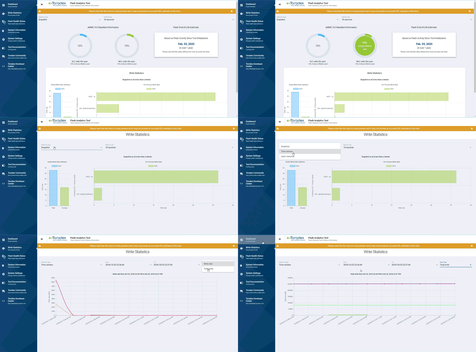
A glimpse of how the UI looks is presented above, With it, I invite you to test-drive it firsthand and tell us what you think about it.
Conclusion
Estimating the flash lifespan can be as simple as calculating from the block size formula given under Flash Health, or as complex as implementing the tools and generating the models needed to estimate a device’s lifetime in seconds. You can choose how much effort to put into it depending on your product’s use case, selecting only the important elements as summarized in Figure 16. Regardless, this is invaluable information.
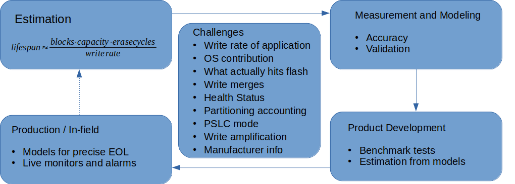
The complex approach offers some benefits over the simpler calculation. In addition to the more precise result, you can also deploy a version of your tool to production to obtain even more precise end-of-life data. This also provides you with monitoring capabilities and the ability to triggers alarms for more predictive maintenance. In the end, a range of low-level and high-level tools, including Micron’s emmcparm, mmc-utils and the Toradex Flash Analytics Tool can all ease your efforts in creating reliable solutions. I hope you’ve had a good time reading this blog post.

Jean-Luc started CNX Software in 2010 as a part-time endeavor, before quitting his job as a software engineering manager, and starting to write daily news, and reviews full time later in 2011.
Support CNX Software! Donate via cryptocurrencies, become a Patron on Patreon, or purchase goods on Amazon or Aliexpress


