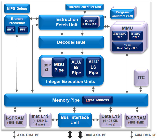
MIPS has recently unveiled the I7200 multi-threaded multi-core processor for advanced LTE/5G communications and networking SoCs, which also happens to be the first MIPS core based on the new nanoMIPS 32-bit ISA.
nanoMIPS is a variable instruction length ISA consisting of 16/32/48-bit instructions and various other optimizations that enables performance in the smallest code size.

MIPS I7200 core features:
- 32-bit nanoMIPS Instruction Set Architecture with MIPS DSP ASE optimized instruction set extensions for integer DSP and 32-bit SIMD operations
- Balanced, 9-stage, dual-issue pipeline with Vertical Multi-Threading (VMT)
- Superscalar on a single thread per cycle
- Zero overhead context switching – can switch threads every clock cycle
- Implements MIPS MT ASE – can implement up to 3 fully OS visible Virtual Processor Elements (VPEs) per core, and up to 9 lightweight thread contexts (TCs) per core, assignable to the VPEs
- Configurable memory subsystem
- Support for caches, tightly coupled ScratchPad RAM (SPRAM), or both
L1 caches – 4-way set associative - 0-128KB each of instruction and data cache with MPU
- 0-64KB each with full TLB-based MMU
- ScratchPad RAM (SPRAM)
- Deterministic low latency instruction/data access and/or high performance data processing and movement outside of standard cached memory hierarchy (e.g. DMA directly into a core’s local D-SPRAM via 128b AXI-4 interface)
- 0-1MB each for instructions, data, or unified SPRAM implementations, with Unified being sharable across CPUs in cluster
- Support for caches, tightly coupled ScratchPad RAM (SPRAM), or both
- Configurable memory management
- Full TLB-based Memory Management Unit (MMU) for Linux and other virtual memory based operating systems
- Simpler, deterministic direct memory access with (up to) 32 region Memory Protection Unit (MPU) for use with Real Time Operating Systems (RTOSs) and bare metal programming

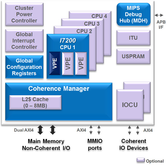
Up to four MIPS I7200 cores and up to 2 hardware I/O coherency unit (IOCLUs) can be integrated in a SoC through the coherence manager.
The company also provided some benchmarks for
- One thread – 4.6 CoreMark/MHz; 2.3 DMIPS/MHz
- Two threads – 5.9 CoreMark/MHz; 2.65 DMIPS/MHz
TSMC 28HPM and TSMC 16FF+ appear to be the manufacturing processes of choice with the latter enabling 2.1 GHz (typical) / 1.7 GHz (worst case) frequencies. The 1.7 GHz design comes with a 0.27mm2 area, 150mW power consumption, and a CoreMark score greater than 40,000 points. The I7200 is said to deliver 50% higher performance in less than 20% area increase than the previous generation from MIPS.
The production released version of the IP core is available immediately for licensing, but we did not get quote from silicon vendors in the press release. We however do know software company are involved with Express Logic providing support for X-Ware IoT Platform powered by the ThreadX RTOS, Imperas Software offering “Imperas and OVP simulators, virtual platforms, and debug and analysis solutions”, as well as Mentor porting Nucleus OS to MIPS I7200 core.
You may want to visit the product page for further information, including download links to the datasheet and a programmer’s guide.

Jean-Luc started CNX Software in 2010 as a part-time endeavor, before quitting his job as a software engineering manager, and starting to write daily news, and reviews full time later in 2011.
Support CNX Software! Donate via cryptocurrencies, become a Patron on Patreon, or purchase goods on Amazon or Aliexpress


