So yesterday, I wrote about some of the new features of Intel Gemini Lake processors like native HDMI 2.0, 4-wide pipeline, 10-bit VP9, and possible built-in 802.11ac wireless controller. I went to bed, and somehow this morning I woke up with something that looks like Gemini Lake (GLK) block diagram, and a few more details.
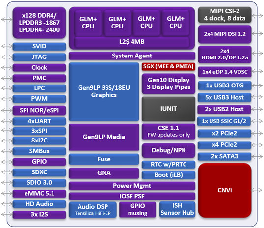 So we indeed have HDMI 2.0 output, as well as DP 1.2a and eDP 1.4, and an embedded wireless controller via the CNVi (Connectivity Integration Architecture) block for WiFi’s MAC and Bluetooth’s MAC + Baseband modem. We’ll have plenty of USB 3.0 host interfaces, and the usual PCIe and SATA 3 interfaces. Still no UFS support, but eMMC 5.1 is supported, as well as x128 DDR4, LPDDR3 and LPDDR4 memory up to 2400 MHz (No ECC support). Cache size is confirmed to be 4MB for up to four GoldMont Plus (GLM+) cores, which combined with the wider pipeline (4 vs 3) will contribute to 10% to 15% better CPU performance compared to Apollo Lake. The Gen9LP GPU in GLK processors will come with up to 18 execution unit.
Another difference will be the update of GMM speech acceleration engine to the GNA version of the SIP with support for DNN (Dynamic Neural Networks) algorithms that could be used for applications such as Microsoft Cortana.

Jean-Luc started CNX Software in 2010 as a part-time endeavor, before quitting his job as a software engineering manager, and starting to write daily news, and reviews full time later in 2011.
Support CNX Software! Donate via cryptocurrencies, become a Patron on Patreon, or purchase goods on Amazon or Aliexpress