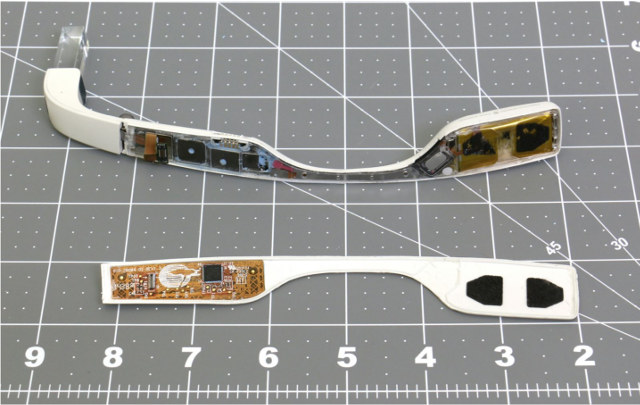
I’ve never been a fan of Google Glass for consumer applications, and the company has apparently more or less given up on this market, but instead they are now focusing on the enterprise market according to Google Glass 2 (codenamed AR4-GG1) photos and a user’s manual released on the FCC website.

The user’s manual lists some of the key external components including a power button, a display with its button to take pictures or shot videos, a touchpad along the flat area on the side to control the display using taps and gestures.

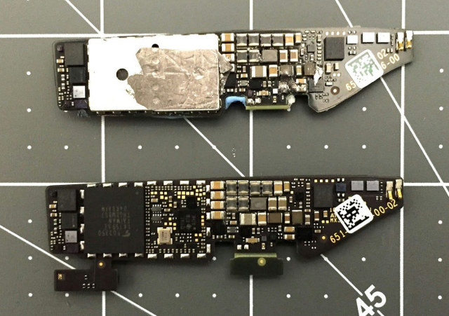
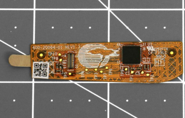
Although not really sharp, the internal pictures allow to have a look at the main electronic components featured in the device, and David Anders analyzed the pictures and found the following ICs:
- Toshiba THGBMBG7D4LBAIW that should be a 16GB eMMC flash
- Texas Instruments TUSB1211 USB 2.0 ULPI PHY transceiver
- Touchpad area with Cypress logo and a 48-pin chip that could be part of TrueTouch CYTT21X/31X family

Mashable also reports that the new version of the glasses features a larger glass prism, a faster Intel Atom processor, and 5 GHz Wi-Fi.

Jean-Luc started CNX Software in 2010 as a part-time endeavor, before quitting his job as a software engineering manager, and starting to write daily news, and reviews full time later in 2011.
Support CNX Software! Donate via cryptocurrencies, become a Patron on Patreon, or purchase goods on Amazon or Aliexpress


