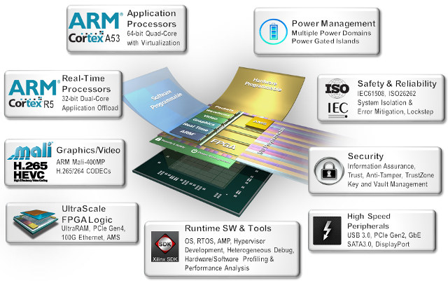
Xilinx Zynq-7000 dual core Cortex A9 + FPGA SoC family was announced in 2012, and provides a wide range of SoC with features and price range, and led to low cost ARM + FPGA such as ZedBoard, and more recently Parallela and MYiR Z-Turn boards. The company unveiled its successor with Zynq UltraScale+ MPSoC providing five times more performance per watt, with four ARM Cortex A53 cores, two ARM Cortex R5 real-time MCU cores, a Mali-400MP GPU, an UltraScale FPGA fabric manufactured with 16nm FinFET+ process.
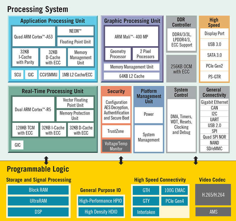
 There are two main sub-families in Zynq Ultrascale+ MPSoC for “smarter control & vision”, and “smarter network”. Both share the same processing systems (CPU, GPU, MCU, Peripherals, Security), but the networking family has beefier FPGAs, and lacks the H.264/H.265 video processing unit found in the control & vision version:
- Processing Systems
- Processor – Quad ARM Cortex A53 MPCore up to 1.3GHz
- Real-time Processor – Dual ARM Cortex-R5 MPCore up to 600MHz
- GPU – Mali-400MP2 up to 466MHz
- External Memory I/F – DDR4, LPDDR4, DDR3, DDR3L, LPDDR3, 2x Quad-SPI, NAND
- High-Speed Connectivity – 2x USB3.0, SATA 3.0, DisplayPort, 4x Tri-mode Gigabit Ethernet, PCIe Gen2x4
- General Connectivity – 2xUSB 2.0, 2x SD/SDIO, 2x UART, 2x CAN 2.0B, 2x I2C, 2x SPI, 4x 32b GPIO
- Security – AES, RSA, and SHA
- AMS System Monitor – 10-bit, 1 MSPS– Temperature, Voltage, and Current Monitor
- Programmable Logic
- FPGA
- Control & Vision (C&V) – Up to 485K Effective LEs, 405K Logic Cells, 1,728 DSP Slices, 6.2 Mb distributed RAM, 11.2 Mb BlockRAM, 27 Mb UltraRAM
- Networking (N) – Up to 1,095K Effective LEs, 920K Logic Cells, 3,528 DSP Slices, 11 Mb distributed RAM, 34.6 Mb BlockRAM, 36 Mb UltraRAM
- PCI Express Interface – Gen4 x8; Gen3 x16
- 1x Video Codec Unit (C&V only) – H.264/H.265 up to 4Kx2Kp60 or 8Kx4Kp15
- Serial Transceiver – C&V: 28 up to 16 Gb/s; N: 76 up to 33 Gb/s
- Analog Mixed Signal (AMS) – System Monitor—10-bit, 1 MSPS ADCs with 17 Differential Inputs, Power supply line voltage monitoring & JTAG, PMBUS, I2C support
- FPGA
The processing systems and programmable logic are interfaced via 128-bit AMBA AXI4 interfaces.

There are 5 parts for Control and Vision (XCZU2, XCZU3, XCZU4, XCZU5, and XCZU7), and 6 parts (XCZU6, XCZU9, XCZU11, XCZU15, XCZU1 and XCZU19) for Network, and even more if you include different packaging options. SKU details and nomenclature can be found in the product selection guide.
The Cortex A53 cores will run Linux, Cortex R5 cores FreeRTOS, and design tools include Vivado Design Suite, Xilinx SDK, and PetaLinux SDK. Zynq UltraScale+ MPSoCs can be used for connected control/machine-to-machine applications for manufacturing, 2D/3D vision application (video-processing, object detection…), wired and wireless networking, and data centers.
I could not find any availability information from Xilinx, but LinuxGizmos reports that “early access to the UltraScale+ processors starts in the second quarter, with samples coming later this year, and volume production due in 2016”.
Visit Xilinx Zynq UltraScale+ MPSoC page for more information.

Jean-Luc started CNX Software in 2010 as a part-time endeavor, before quitting his job as a software engineering manager, and starting to write daily news, and reviews full time later in 2011.
Support CNX Software! Donate via cryptocurrencies, become a Patron on Patreon, or purchase goods on Amazon or Aliexpress


