What’s a WPU? It stands for Wearable Processor Unit, and as you may guess it’s a processor specifically designed to be used in wearables such as smartwatches or fitness trackers. Currently, many wearables are based on application processors that are used in smartphones (e.g. Galaxy Gear), and lower-end versions are based on standard low power MCUs (e.g. Pebble), but none of them are actually based on SoC specifically designed for wearables, and analysts are asserting that new types of SoC are definitely needed if companies are to provide wearables with the battery life and features consumers want. Ineda Systems Dhanush WPU is not the first Wearable SoC announced, as for instance AllWinner mentioned their WX quad-core SoC for Wearables should become available in Q4 2014 in their roadmap, and Mediatek vaguely unveiled their Aster SoC at CES 2014, but it’s the first that I know of where we’ve got most of the details announced.

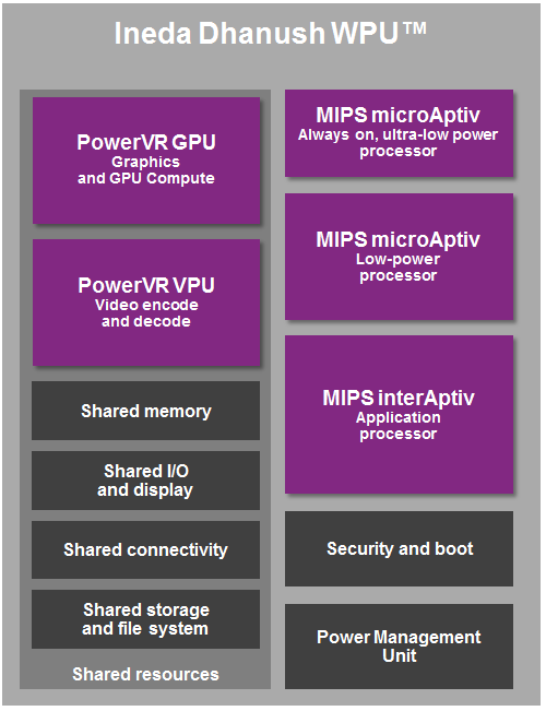
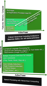
Now that block diagram looks interesting… In order to achieve maximum battery life, Ineda has adopted a sort of “big.LITTLE processing” concept to wearables which they call Hierarchical Computing Architecture (HCA) with up to 3 cores offering three levels of performance and power consumption: MIPS microAptiv (always on for sensors, ultra-low power), MIPS microAptive (low power), and MIPS interAptive application processor.
Dhanush SoCs actually comes in four flavors with only one core, 2-level HCA or 3-level HCA:

- Dhanush Nano
- microAptiv MCU
- Memory – On-chip SRAM
- For werable devices that require MCU class of compute and memory footprint such as smartbands
- Dhanush Micro (2-level HCA)
- Ultra low power, always-on microAptiv MCU for sensors
- “high performance” low power microAptiv MCU
- Memory – On-chip SRAM
- Typical application would be a Linux based or RTOS based smartwatch.
- Dhanush Optima (2-level HCA)
- Ultra low power, always-on microAptiv MCU for sensors
- “high performance” low power microAptiv MCU
- Memory – On-chip SRAM + LPDDR2
- For Linux based smartwatches requiring more features
- Dhanush Advanced (3-level HCA)
- Ultra low power, always-on microAptiv MCU for sensors
- “high performance” low power microAptiv MCU
- Dual-core, multi-threaded interAptiv CPU
- Multimedia – PowerVR GPU and VPU for video encode/decode
- Memory – On-chip SRAM + LPDDR2
- For more advanced, high-end wearables that require high-resolution rendering, handle complex image/video processing via GPU compute and also support low power video recording and playback. Typical applications would be Android smartwatches or smart glasses.
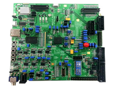
Ineda Systems can provide two SHASTRA development kit:
- SHASTRA-A for Dhanush Advanced (INCDHAD1) which can also be used to evaluate Dhanush Optima
- SHASTRA-M for Dhanush Micro (INCDHMC1) which can also be used to evaluate Dhanush Nano

The boards come with a software development kit (SDK) including a unified development environment (OS, Drivers, Services, APIs, Sample Applications), integrated resource & power management, a GUI framework, user guides, tools & build utilities, and power profiling tools. There are two variants of SHASTRA SDK, one for evaluation, and one for product development.
Dhanush Advanced (INCDHAD1) and Micro (INCDHMC1) are now sampling for early customers. The production status of Nano and Optima versions are not been disclosed. I’d guess that means actual products may retail by the end of the year at the earliest. You can find more information on Ineda Systems’ Dhanush WPU page, as well as Imagination Technologies Blog.

Jean-Luc started CNX Software in 2010 as a part-time endeavor, before quitting his job as a software engineering manager, and starting to write daily news, and reviews full time later in 2011.
Support CNX Software! Donate via cryptocurrencies, become a Patron on Patreon, or purchase goods on Amazon or Aliexpress


